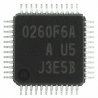
M30260F6AGP#U5A Renesas Electronics America, M30260F6AGP#U5A Datasheet - Page 341

M30260F6AGP#U5A
Manufacturer Part Number
M30260F6AGP#U5A
Description
IC M16C MCU FLASH 48K 48LQFP
Manufacturer
Renesas Electronics America
Series
M16C™ M16C/Tiny/26r
Datasheet
1.M30260F3AGPU5A.pdf
(354 pages)
Specifications of M30260F6AGP#U5A
Core Processor
M16C/60
Core Size
16-Bit
Speed
20MHz
Connectivity
I²C, IEBus, SIO, UART/USART
Peripherals
DMA, PWM, Voltage Detect, WDT
Number Of I /o
39
Program Memory Size
48KB (48K x 8)
Program Memory Type
FLASH
Ram Size
2K x 8
Voltage - Supply (vcc/vdd)
2.7 V ~ 5.5 V
Data Converters
A/D 12x10b
Oscillator Type
Internal
Operating Temperature
-20°C ~ 85°C
Package / Case
48-LQFP
Cpu Family
R8C
Device Core Size
16b
Frequency (max)
20MHz
Interface Type
UART
Total Internal Ram Size
2KB
# I/os (max)
39
Number Of Timers - General Purpose
8
Operating Supply Voltage (typ)
3.3/5V
Operating Supply Voltage (max)
5.5V
Operating Supply Voltage (min)
3V
On-chip Adc
12-chx10-bit
Instruction Set Architecture
CISC
Operating Temp Range
-20C to 85C
Operating Temperature Classification
Commercial
Mounting
Surface Mount
Pin Count
48
Package Type
LQFP
Package
48LQFP
Family Name
R8C
Maximum Speed
20 MHz
Operating Supply Voltage
3.3|5 V
Data Bus Width
16 Bit
Number Of Programmable I/os
39
Number Of Timers
8
For Use With
R0K33026AS000BE - KIT DEV EVALUATION M16C/26A
Lead Free Status / RoHS Status
Lead free / RoHS Compliant
Eeprom Size
-
Lead Free Status / Rohs Status
Compliant
Available stocks
Company
Part Number
Manufacturer
Quantity
Price
Part Number:
M30260F6AGP#U5AM30260F6AGP#D3
Manufacturer:
Renesas Electronics America
Quantity:
10 000
Part Number:
M30260F6AGP#U5AM30260F6AGP#U3
Manufacturer:
Renesas Electronics America
Quantity:
10 000
Part Number:
M30260F6AGP#U5AM30260F6AGP#U3A
Manufacturer:
Renesas Electronics America
Quantity:
10 000
- Current page: 341 of 354
- Download datasheet (4Mb)
R
R
M
e
E
1
. v
J
6
0
C
19.13.14 Definition of Programming/Erasure Times
19.13.15 Flash Memory Version Electrical Characteristics 10,000 E/W cycle products (U7, U9)
19.13.16 Boot Mode
2
9
0 .
B
2 /
"Number of programs and erasure" refers to the number of erasure per block.
If the number of program and erasure is n (n=100 1,000 10,000) each block can be erased n times.
For example, if a 2K byte block A is erased after writing 1 word data 1024 times, each to a different
address, this is counted as one program and erasure. However, data cannot be written to the same
adrress more than once without erasing the block. (Rewrite prohibited)
When Block A or B E/W cycles exceed 100, select one wait state per block access. When FMR17 is set
to "1", one wait state is inserted per access to Block A or B - regardless of the value of PM17. Wait state
insertion during access to all other blocks, as well as to internal RAM, is controlled by PM17 - regardless
of the setting of FMR17.
To use the limited number of erasure efficiently, write to unused address within the block instead of
rewite. Erase block only after all possible address are used. For example, an 8-word program can be
written 128 times before erase becomes necessary.
Maintaining an equal number of erasure between Block A and B will also improve efficiency.
We recommend keeping track of the number of times erasure is used.
An indeterminate value is sometimes output in the I/O port until the internal power supply becomes stable
when "H" is applied to the CNV
When setting the CNV
When the CNV
0
0
6
2
A
0
F
2
e
G
0 -
b
(1) Apply an "L" signal to the RESET pin and the CNV
(2) Bring V
(3) Apply an "H" signal to the CNV
(4) Apply an "H" signal to the RESET pin.
o r
1 .
2
0
u
, 5
0
p
2
(
0
M
0
7
1
SS
6
C
CC
page 322
pin is “H” and RESET pin is “L”, P6
2 /
6
to more than 2.7V, and wait at least 2msec. (Internal power supply stable waiting time)
, A
SS
M
pin to "H", the following procedure is required:
1
f o
6
C
3
2
2 /
SS
9
6
, B
pin and "L" is applied to the RESET pin.
____________
____________
M
1
6
SS
C
2 /
pin.
6
) T
7
pin is connected to the pull-up resister.
SS
_____________
pin.
19. Usage Notes
Related parts for M30260F6AGP#U5A
Image
Part Number
Description
Manufacturer
Datasheet
Request
R

Part Number:
Description:
KIT STARTER FOR M16C/29
Manufacturer:
Renesas Electronics America
Datasheet:

Part Number:
Description:
KIT STARTER FOR R8C/2D
Manufacturer:
Renesas Electronics America
Datasheet:

Part Number:
Description:
R0K33062P STARTER KIT
Manufacturer:
Renesas Electronics America
Datasheet:

Part Number:
Description:
KIT STARTER FOR R8C/23 E8A
Manufacturer:
Renesas Electronics America
Datasheet:

Part Number:
Description:
KIT STARTER FOR R8C/25
Manufacturer:
Renesas Electronics America
Datasheet:

Part Number:
Description:
KIT STARTER H8S2456 SHARPE DSPLY
Manufacturer:
Renesas Electronics America
Datasheet:

Part Number:
Description:
KIT STARTER FOR R8C38C
Manufacturer:
Renesas Electronics America
Datasheet:

Part Number:
Description:
KIT STARTER FOR R8C35C
Manufacturer:
Renesas Electronics America
Datasheet:

Part Number:
Description:
KIT STARTER FOR R8CL3AC+LCD APPS
Manufacturer:
Renesas Electronics America
Datasheet:

Part Number:
Description:
KIT STARTER FOR RX610
Manufacturer:
Renesas Electronics America
Datasheet:

Part Number:
Description:
KIT STARTER FOR R32C/118
Manufacturer:
Renesas Electronics America
Datasheet:

Part Number:
Description:
KIT DEV RSK-R8C/26-29
Manufacturer:
Renesas Electronics America
Datasheet:

Part Number:
Description:
KIT STARTER FOR SH7124
Manufacturer:
Renesas Electronics America
Datasheet:

Part Number:
Description:
KIT STARTER FOR H8SX/1622
Manufacturer:
Renesas Electronics America
Datasheet:

Part Number:
Description:
KIT DEV FOR SH7203
Manufacturer:
Renesas Electronics America
Datasheet:


