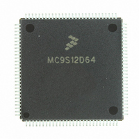
MC9S12D64VPVE Freescale Semiconductor, MC9S12D64VPVE Datasheet - Page 61

MC9S12D64VPVE
Manufacturer Part Number
MC9S12D64VPVE
Description
IC MCU 64K FLASH 25MHZ 112-LQFP
Manufacturer
Freescale Semiconductor
Series
HCS12r
Specifications of MC9S12D64VPVE
Core Processor
HCS12
Core Size
16-Bit
Speed
25MHz
Connectivity
CAN, I²C, SCI, SPI
Peripherals
PWM, WDT
Number Of I /o
91
Program Memory Size
64KB (64K x 8)
Program Memory Type
FLASH
Eeprom Size
1K x 8
Ram Size
4K x 8
Voltage - Supply (vcc/vdd)
2.35 V ~ 5.25 V
Data Converters
A/D 8x10b
Oscillator Type
Internal
Operating Temperature
-40°C ~ 105°C
Package / Case
112-LQFP
Lead Free Status / RoHS Status
Lead free / RoHS Compliant
Available stocks
Company
Part Number
Manufacturer
Quantity
Price
Company:
Part Number:
MC9S12D64VPVE
Manufacturer:
Freescale Semiconductor
Quantity:
10 000
Company:
Part Number:
MC9S12D64VPVER
Manufacturer:
Freescale Semiconductor
Quantity:
10 000
MC9S12DJ64 Device User Guide — V01.20
2.3.30 PJ6 / KWJ6 / SDA / RXCAN0 — PORT J I/O Pin 6
PJ6 is a general purpose input or output pin. It can be configured to generate an interrupt causing the MCU
to exit STOP or WAIT mode. It can be configured as the serial data pin SDA of the IIC module. It can be
configured as the receive pin RXCAN of the Freescale Scalable Controller Area Network controller 0
(CAN0).
2.3.31 PJ[1:0] / KWJ[1:0] — Port J I/O Pins [1:0]
PJ1 and PJ0 are general purpose input or output pins. They can be configured to generate an interrupt
causing the MCU to exit STOP or WAIT mode.
2.3.32 PK7 / ECS / ROMCTL — Port K I/O Pin 7
PK7 is a general purpose input or output pin. During MCU expanded modes of operation, this pin is used
as the emulation chip select output (ECS). During MCU expanded modes of operation, this pin is used to
enable the Flash EEPROM memory in the memory map (ROMCTL). At the rising edge of RESET, the
state of this pin is latched to the ROMON bit. For a complete list of modes refer to 4.2 Chip Configuration
Summary.
2.3.33 PK[5:0] / XADDR[19:14] — Port K I/O Pins [5:0]
PK5-PK0 are general purpose input or output pins. In MCU expanded modes of operation, these pins
provide the expanded address XADDR[19:14] for the external bus.
2.3.34 PM7 — Port M I/O Pin 7
PM7 is a general purpose input or output pin.
2.3.35 PM6 — Port M I/O Pin 6
PM6 is a general purpose input or output pin.
2.3.36 PM5 / TXCAN0 / SCK0 — Port M I/O Pin 5
PM5 is a general purpose input or output pin. It can be configured as the transmit pin TXCAN of the
Freescale Scalable Controller Area Network controller 0 (CAN0). It can be configured as the serial clock
pin SCK of the Serial Peripheral Interface 0 (SPI0).
2.3.37 PM4 / RXCAN0 / MOSI0 — Port M I/O Pin 4
PM4 is a general purpose input or output pin. It can be configured as the receive pin RXCAN of the
Freescale Scalable Controller Area Network controller 0 (CAN0). It can be configured as the master output
(during master mode) or slave input pin (during slave mode) MOSI for the Serial Peripheral Interface 0
(SPI0).
61


