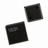
P87C51MC2BA/02,529 NXP Semiconductors, P87C51MC2BA/02,529 Datasheet - Page 14

P87C51MC2BA/02,529
Manufacturer Part Number
P87C51MC2BA/02,529
Description
IC 80C51 MCU 96K OTP 44-PLCC
Manufacturer
NXP Semiconductors
Series
87Cr
Datasheet
1.P87C51MB2BA02529.pdf
(36 pages)
Specifications of P87C51MC2BA/02,529
Program Memory Type
OTP
Program Memory Size
96KB (96K x 8)
Package / Case
44-PLCC
Core Processor
8051
Core Size
8-Bit
Speed
24MHz
Connectivity
EBI/EMI, SPI, UART/USART
Peripherals
POR, PWM, WDT
Number Of I /o
34
Ram Size
3K x 8
Voltage - Supply (vcc/vdd)
2.7 V ~ 5.5 V
Oscillator Type
Internal
Operating Temperature
0°C ~ 70°C
Processor Series
P87C5x
Core
80C51
Data Bus Width
8 bit
Data Ram Size
3 KB
Interface Type
SPI, UART
Maximum Clock Frequency
24 MHz
Number Of Programmable I/os
34
Number Of Timers
3
Operating Supply Voltage
2.7 V to 5.5 V
Maximum Operating Temperature
+ 70 C
Mounting Style
SMD/SMT
3rd Party Development Tools
PK51, CA51, A51, ULINK2
Minimum Operating Temperature
0 C
Cpu Family
87C
Device Core
80C51
Device Core Size
8b
Frequency (max)
24MHz
Total Internal Ram Size
3KB
# I/os (max)
34
Number Of Timers - General Purpose
3
Operating Supply Voltage (typ)
3.3/5V
Operating Supply Voltage (max)
5.5V
Operating Supply Voltage (min)
2.7V
Instruction Set Architecture
CISC
Operating Temp Range
0C to 70C
Operating Temperature Classification
Commercial
Mounting
Surface Mount
Pin Count
44
Package Type
PLCC
Lead Free Status / RoHS Status
Lead free / RoHS Compliant
For Use With
OM10064 - EMULATOR 80C51 PDS51-MK2
Eeprom Size
-
Data Converters
-
Lead Free Status / Rohs Status
Compliant
Other names
568-1244-5
935273219529
P87C51MC2BA/02-S
935273219529
P87C51MC2BA/02-S
Available stocks
Company
Part Number
Manufacturer
Quantity
Price
Company:
Part Number:
P87C51MC2BA/02,529
Manufacturer:
NXP Semiconductors
Quantity:
10 000
Table 4:
[1]
[2]
[3]
[4]
[5]
[6]
Name
S1STAT
SPCTL
SPCFG
SPDAT
SP
SPE
TCON
T2CON
T2MOD
TH0
TH1
TH2
TL0
TL1
TL2
TMOD
WDTRST
WDCON
SFRs are bit addressable.
SFRs are modified from or added to the 80C51 SFRs.
Extended SFRs accessed by preceding the instruction with MX escape (opcode A5h).
Power on reset is 10H. Other reset is 00H.
BRGR1 and BRGR0 must only be written if BRGEN in BRGCON SFR is ‘0’. If any of them is written if BRGEN = 1, result is unpredictable.
The unimplemented bits (labeled ‘-’) in the SFRs are X’s (unknown) at all times. ‘1’s should not be written to these bits, as they may be used for other purposes in future
derivatives. The reset values shown for these bits are ‘0’s although they are unknown when read.
[2]
[1]
[2]
[2]
[1] [2]
[2]
[2]
[2]
[2]
[2]
xxxxxxxxxxxxxxxxxxxxx xxxxxxxxxxxxxxxxxxxxxxxxxxxxxx xxxxx xxxxxxxxxxxxxxxxxxxxxxxxxxxxxxxxxxxxxxxxxxxxxxxxxx xxxxxxxx
xxxxxxxxxxxxxxxxxxxxxxxxx xxxxxxxxxxxxxxxxxxxx xxx
Special Function Registers
Description
Serial Port 1 Status
SPI Control Register
SPI Configuration Register
SPI Data
Stack Pointer (or Stack Pointer
LOW Byte When EDATA
Supported)
Stack Pointer HIGH
Timer Control Register
Timer2 Control Register
Timer2 Mode Control
Timer 0 HIGH
Timer 1 HIGH
Timer 2 HIGH
Timer 0 LOW
Timer 1 LOW
Timer 2 LOW
Timer 0 and 1 Mode
Watchdog Timer Reset
Watchdog Timer Control
…continued
Bit address 8F
SFR
Addr.
84H
E2H
E1H
E3H
81H
FBH
88H
C8H
C9H
8CH
8DH
CDH
8AH
8BH
CCH
89H
A6H
8FH
[3]
[3]
[3]
Bit functions and addresses
MSB
DBMOD_1 INTLO_1
SSIG
SPIF
TF1
CF
TF2
-
GATE
-
SPEN
SPWCOL -
8E
TR1
CE
EXF2
-
C/T
-
CIDIS_1 DBISEL1 FE_1
DORD
8D
TF0
CD
RCLK
ENT2
M1
-
MSTR
-
8C
TR0
CC
TCLK
TF2DE
M0
-
CPOL
-
8B
IE1
CB
EXEN2
T2GATE T2PWME T2OE
GATE
-
BR_1
CPHA
-
8A
IT1
CA
TR2
C/T
WDPRE2 WDPRE1 WDPRE0 00H
OE_1
PSC1
-
89
IE0
C9
C/T2
M1
LSB
STINT_1
PSC0
-
88
IT0
C8
CP/RL2
DCEN
M0
Reset
value
00H
00H
00H
00H
07H
00H
00H
00H
00H
00H
00H
00H
00H
00H
00H
00H
FFH
[6]
[6]
[6]
[6]
[6]


