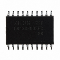
Z8F0813SH005EC Zilog, Z8F0813SH005EC Datasheet - Page 110

Z8F0813SH005EC
Manufacturer Part Number
Z8F0813SH005EC
Description
IC Z8 ENCORE MCU FLASH 8K 20SOIC
Manufacturer
Zilog
Series
Encore!® XP®r
Datasheet
1.Z8F0813PH005SC.pdf
(227 pages)
Specifications of Z8F0813SH005EC
Core Processor
Z8
Core Size
8-Bit
Speed
5MHz
Connectivity
IrDA, UART/USART
Peripherals
Brown-out Detect/Reset, LED, POR, PWM, WDT
Number Of I /o
16
Program Memory Size
8KB (8K x 8)
Program Memory Type
FLASH
Ram Size
1K x 8
Voltage - Supply (vcc/vdd)
2.7 V ~ 3.6 V
Oscillator Type
Internal
Operating Temperature
-40°C ~ 105°C
Package / Case
20-SOIC (7.5mm Width)
Lead Free Status / RoHS Status
Contains lead / RoHS non-compliant
Eeprom Size
-
Data Converters
-
Other names
269-3721
- Current page: 110 of 227
- Download datasheet (3Mb)
PS025203-0405
External Driver Enable
devices on the multi-node network. The following three MULTIPROCESSOR modes are
available in hardware:
•
•
•
These modes are selected with MPMD[1:0] in the UART Control 1 Register. For all mul-
tiprocessor modes, bit MPEN of the UART Control 1 Register must be set to 1.
The first scheme is enabled by writing
address bytes cause an interrupt, while data bytes never cause an interrupt. The interrupt
service routine must manually check the address byte that caused triggered the interrupt. If
it matches the UART address, the software clears MPMD[0]. Each new incoming byte
interrupts the CPU. The software is responsible for determining the end of the frame. It
checks for the end-of-frame by reading the MPRX bit of the UART Status 1 Register for
each incoming byte. If MPRX=1, a new frame has begun. If the address of this new frame
is different from the UART’s address, MPMD[0] must be set to 1 causing the UART inter-
rupts to go inactive until the next address byte. If the new frame’s address matches the
UART’s, the data in the new frame is processed as well.
The second scheme requires the following: set MPMD[1:0] to
address into the UART Address Compare Register. This mode introduces additional hard-
ware control, interrupting only on frames that match the UART’s address. When an
incoming address byte does not match the UART’s address, it is ignored. All successive
data bytes in this frame are also ignored. When a matching address byte occurs, an inter-
rupt is issued and further interrupts now occur on each succesive data byte. When the first
data byte in the frame is read, the NEWFRM bit of the UART Status 1 Register is asserted.
All successive data bytes have NEWFRM=0. When the next address byte occurs, the hard-
ware compares it to the UART’s address. If there is a match, the interrupts continues and
the NEWFRM bit is set for the first byte of the new frame. If there is no match, the UART
ignores all incoming bytes until the next address match.
The third scheme is enabled by setting MPMD[1:0] to
address into the UART Address Compare Register. This mode is identical to the second
scheme, except that there are no interrupts on address bytes. The first data byte of each
frame remains accompanied by a NEWFRM assertion.
The UART provides a Driver Enable (DE) signal for off-chip bus transceivers. This fea-
ture reduces the software overhead associated with using a GPIO pin to control the trans-
ceiver when communicating on a multi-transceiver bus, such as RS-485.
Driver Enable is an active High signal that envelopes the entire transmitted data frame
including parity and Stop bits as illustrated in Figure 14. The Driver Enable signal asserts
when a byte is written to the UART Transmit Data register. The Driver Enable signal
Interrupt on all address bytes
Interrupt on matched address bytes and correctly framed data bytes
Interrupt only on correctly framed data bytes
P R E L I M I N A R Y
01b
to MPMD[1:0]. In this mode, all incoming
11b
Z8 Encore!
and by writing the UART’s
10B
Product Specification
and write the UART’s
®
Z8F0823 Series
UART
93
Related parts for Z8F0813SH005EC
Image
Part Number
Description
Manufacturer
Datasheet
Request
R

Part Number:
Description:
Communication Controllers, ZILOG INTELLIGENT PERIPHERAL CONTROLLER (ZIP)
Manufacturer:
Zilog, Inc.
Datasheet:

Part Number:
Description:
KIT DEV FOR Z8 ENCORE 16K TO 64K
Manufacturer:
Zilog
Datasheet:

Part Number:
Description:
KIT DEV Z8 ENCORE XP 28-PIN
Manufacturer:
Zilog
Datasheet:

Part Number:
Description:
DEV KIT FOR Z8 ENCORE 8K/4K
Manufacturer:
Zilog
Datasheet:

Part Number:
Description:
KIT DEV Z8 ENCORE XP 28-PIN
Manufacturer:
Zilog
Datasheet:

Part Number:
Description:
DEV KIT FOR Z8 ENCORE 4K TO 8K
Manufacturer:
Zilog
Datasheet:

Part Number:
Description:
CMOS Z8 microcontroller. ROM 16 Kbytes, RAM 256 bytes, speed 16 MHz, 32 lines I/O, 3.0V to 5.5V
Manufacturer:
Zilog, Inc.
Datasheet:

Part Number:
Description:
Low-cost microcontroller. 512 bytes ROM, 61 bytes RAM, 8 MHz
Manufacturer:
Zilog, Inc.
Datasheet:

Part Number:
Description:
Z8 4K OTP Microcontroller
Manufacturer:
Zilog, Inc.
Datasheet:

Part Number:
Description:
CMOS SUPER8 ROMLESS MCU
Manufacturer:
Zilog, Inc.
Datasheet:

Part Number:
Description:
SL1866 CMOSZ8 OTP Microcontroller
Manufacturer:
Zilog, Inc.
Datasheet:

Part Number:
Description:
SL1866 CMOSZ8 OTP Microcontroller
Manufacturer:
Zilog, Inc.
Datasheet:

Part Number:
Description:
OTP (KB) = 1, RAM = 125, Speed = 12, I/O = 14, 8-bit Timers = 2, Comm Interfaces Other Features = Por, LV Protect, Voltage = 4.5-5.5V
Manufacturer:
Zilog, Inc.
Datasheet:

Part Number:
Description:
Manufacturer:
Zilog, Inc.
Datasheet:


