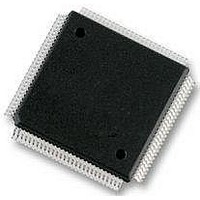
MCF53011CQT240 Freescale Semiconductor, MCF53011CQT240 Datasheet - Page 23

MCF53011CQT240
Manufacturer Part Number
MCF53011CQT240
Description
MCU 32BIT COLDFIRE EMAC 208LQFP
Manufacturer
Freescale Semiconductor
Series
MCF5301xr
Datasheet
1.MCF53010CQT240.pdf
(62 pages)
Specifications of MCF53011CQT240
Core Processor
Coldfire V3
Core Size
32-Bit
Speed
240MHz
Connectivity
EBI/EMI, Ethernet, I²C, MMC, SPI, SSI, UART/USART, USB OTG
Peripherals
DMA, PWM, WDT
Number Of I /o
61
Program Memory Size
16KB (16K x 8)
Program Memory Type
Cache
Ram Size
128K x 8
Voltage - Supply (vcc/vdd)
1.08 V ~ 3.6 V
Oscillator Type
Internal
Operating Temperature
-40°C ~ 85°C
Package / Case
208-LQFP
Processor Series
MCF5301x
Core
ColdFire V3
Data Bus Width
32 bit
Data Ram Size
128 KB
Interface Type
UART, I2C, SPI, SSI, Ethernet
Maximum Clock Frequency
20 MHz to 400 MHz
Number Of Programmable I/os
61
Number Of Timers
8
Operating Supply Voltage
3.6 V
Maximum Operating Temperature
+ 85 C
Mounting Style
SMD/SMT
3rd Party Development Tools
JLINK-CF-BDM26, EWCF
Development Tools By Supplier
M53015EVB, M53017KIT, M53017MOD
Minimum Operating Temperature
- 40 C
Lead Free Status / RoHS Status
Lead free / RoHS Compliant
Eeprom Size
-
Data Converters
-
Lead Free Status / Rohs Status
Lead free / RoHS Compliant
5.4.3
The relationship between SDV
or 3.3V) and EV
5.4.3.1
If EV
connected to the EV
before IV
or there will be high current in the internal ESD protection diodes. The rise times on the power supplies should be slower than
500 us to avoid turning on the internal ESD protection clamp diodes.
5.4.3.2
If IV
impedance state. There is no limit on how long after IV
down. IV
undesired high current in the ESD protection diodes. There are no requirements for the fall times of the power supplies.
The recommended power down sequence is as follows:
Freescale Semiconductor
1.
2.
DD
DD
/PLLV
/SDV
Drop IV
Drop EV
DD
DD
must powered up. IV
should not lag EV
DD
Supply Voltage Sequencing and Separation Cautions
DD
Power Up Sequence
Power Down Sequence
DD
DD
are powered up with IV
In addition to the above filter circuitry, a 0.01 F capacitor is also recommended in parallel
with those shown.
are powered down first, then sense circuits in the I/O pads will cause all output drivers to be in a high
DD
are specified relative to IV
DD
/PLLV
/SDV
/SDV
DD
DD
Board EV
DD
supplies.
to 0 V.
DD
DD
to be in a high impedance state. There is no limit on how long after EV
DD
, SDV
and EV
should not lead the EV
Preliminary—Subject to Change Without Notice
DD
DD
DD
DD
, or PLLV
Figure 9. USB V
at 0 V, then the sense circuits in the I/O pads will cause all pad output drivers
is non-critical during power-up and power-down sequences. Both SDV
DD
MCF5301x Data Sheet, Rev. 5
0 Ω
.
DD
DD
going low by more than 0.4 V during power down or there will be
NOTE
and PLLV
10 µF
DD
, SDV
GND
DD
Power Filter
DD
DD
or PLLV
power down before EV
0.1 µF
DD
by more than 0.4 V during power ramp-up,
Preliminary Electrical Characteristics
USB V
DD
DD
Pin
or SDV
DD
/SDV
DD
must power
DD
powers up
DD
(2.5V
23


