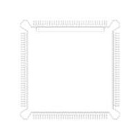
MC68332AMEH20 Freescale Semiconductor, MC68332AMEH20 Datasheet - Page 66

MC68332AMEH20
Manufacturer Part Number
MC68332AMEH20
Description
IC MCU 32BIT 20MHZ 132-PQFP
Manufacturer
Freescale Semiconductor
Series
M683xxr
Specifications of MC68332AMEH20
Core Processor
CPU32
Core Size
32-Bit
Speed
20MHz
Connectivity
EBI/EMI, SCI, SPI, UART/USART
Peripherals
POR, PWM, WDT
Number Of I /o
15
Program Memory Type
ROMless
Ram Size
2K x 8
Voltage - Supply (vcc/vdd)
4.5 V ~ 5.5 V
Oscillator Type
Internal
Operating Temperature
-40°C ~ 125°C
Package / Case
132-QFP
Processor Series
M683xx
Core
CPU32
Data Bus Width
32 bit
Controller Family/series
68K
No. Of I/o's
15
Ram Memory Size
2KB
Cpu Speed
20MHz
No. Of Timers
1
Embedded Interface Type
QSPI, SCI, UART
Digital Ic Case Style
PQFP
Rohs Compliant
Yes
Data Ram Size
2 KB
Interface Type
QSPI, SCI, UART
Maximum Clock Frequency
20 MHz
Number Of Programmable I/os
15
Number Of Timers
16
Maximum Operating Temperature
+ 125 C
Mounting Style
SMD/SMT
Minimum Operating Temperature
- 40 C
Package
132PQFP
Device Core
ColdFire
Family Name
68K/M683xx
Maximum Speed
20 MHz
Operating Supply Voltage
5 V
Lead Free Status / RoHS Status
Lead free / RoHS Compliant
Eeprom Size
-
Program Memory Size
-
Data Converters
-
Lead Free Status / Rohs Status
Lead free / RoHS Compliant
Available stocks
Company
Part Number
Manufacturer
Quantity
Price
Company:
Part Number:
MC68332AMEH20
Manufacturer:
Freescale Semiconductor
Quantity:
135
Company:
Part Number:
MC68332AMEH20
Manufacturer:
Freescale Semiconductor
Quantity:
10 000
6.3 Pin Function
6.4 QSM Registers
6.4.1 Global Registers
QSMCR — QSM Configuration Register
STOP — Stop Enable
66
MOTOROLA
RESET:
STOP
15
0
The following table is a summary of the functions of the QSM pins when they are not configured for gen-
eral-purpose I/O. The QSM data direction register (DDRQS) designates each pin except RXD as an in-
put or output.
QSM registers are divided into four categories: QSM global registers, QSM pin control registers, QSPI
submodule registers, and SCI submodule registers. The QSPI and SCI registers are defined in separate
sections below. Writes to unimplemented register bits have no meaning or effect, and reads from unim-
plemented bits always return a logic zero value.
The module mapping bit of the SIM configuration register (SIMCR) defines the most significant bit
(ADDR23) of the address, shown in each register figure as Y (Y = $7 or $F). This bit, concatenated with
the rest of the address given, forms the absolute address of each register. Refer to the SIM section of
this technical summary for more information about how the state of MM affects the system.
The QSM global registers contain system parameters used by both the QSPI and the SCI submodules.
These registers contain the bits and fields used to configure the QSM.
The QSMCR contains parameters for the QSM/CPU/intermodule bus (IMB) interface.
STOP places the QSM in a low-power state by disabling the system clock in most parts of the module.
The QSMCR is the only register guaranteed to be readable while STOP is asserted. The QSPI RAM is
not readable. However, writes to RAM or any register are guaranteed to be valid while STOP is assert-
ed. STOP can be negated by the CPU and by reset.
0 = Normal QSM clock operation
1 = QSM clock operation stopped
FRZ1
14
0
QSPI Pins
SCI Pins
FRZ0
13
0
12
0
0
Freescale Semiconductor, Inc.
11
For More Information On This Product,
0
0
PCS0/SS
PCS[3:1]
10
0
0
MISO
MOSI
SCK
RXD
TXD
Pin
Go to: www.freescale.com
9
0
0
8
0
0
Transmit
Receive
Master
Master
Master
Master
Master
SUPV
Mode
Slave
Slave
Slave
Slave
Slave
7
1
6
0
0
Serial Data Input to QSPI
Serial Data Output from QSPI
Serial Data Output from QSPI
Serial Data Input to QSPI
Clock Output from QSPI
Clock Input to QSPI
Input: Assertion Causes Mode Fault
Output: Selects Peripherals
Input: Selects the QSPI
Output: Selects Peripherals
None
Serial Data Output from SCI
Serial Data Input to SCI
5
0
0
4
0
0
Pin Function
3
0
0
MC68332TS/D
IARB
$YFFC00
0
MC68332
0
0


