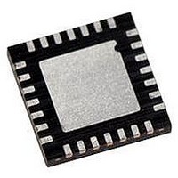
PIC18LF27J53-I/ML Microchip Technology, PIC18LF27J53-I/ML Datasheet - Page 146

PIC18LF27J53-I/ML
Manufacturer Part Number
PIC18LF27J53-I/ML
Description
IC PIC MCU 128KB FLASH 28QFN
Manufacturer
Microchip Technology
Series
PIC® XLP™ 18Fr
Datasheets
1.PIC18LF24J10-ISS.pdf
(32 pages)
2.PIC18F26J13-ISS.pdf
(496 pages)
3.PIC18F26J53-ISS.pdf
(586 pages)
4.PIC18F26J53-ISS.pdf
(12 pages)
Specifications of PIC18LF27J53-I/ML
Core Size
8-Bit
Program Memory Size
128KB (64K x 16)
Core Processor
PIC
Speed
48MHz
Connectivity
I²C, LIN, SPI, UART/USART, USB
Peripherals
Brown-out Detect/Reset, POR, PWM, WDT
Number Of I /o
22
Program Memory Type
FLASH
Ram Size
3.8K x 8
Voltage - Supply (vcc/vdd)
2 V ~ 2.75 V
Data Converters
A/D 10x10b/12b
Oscillator Type
Internal
Operating Temperature
-40°C ~ 85°C
Package / Case
*
Controller Family/series
PIC18
Cpu Speed
48MHz
Digital Ic Case Style
QFN
Supply Voltage Range
1.8V To 3.6V
Embedded Interface Type
I2C, SPI, USART
Rohs Compliant
Yes
Lead Free Status / RoHS Status
Lead free / RoHS Compliant
Eeprom Size
-
Lead Free Status / RoHS Status
Lead free / RoHS Compliant, Lead free / RoHS Compliant
Available stocks
Company
Part Number
Manufacturer
Quantity
Price
Company:
Part Number:
PIC18LF27J53-I/ML
Manufacturer:
ATMEL
Quantity:
101
- PIC18LF24J10-ISS PDF datasheet
- PIC18F26J13-ISS PDF datasheet #2
- PIC18F26J53-ISS PDF datasheet #3
- PIC18F26J53-ISS PDF datasheet #4
- Current page: 146 of 496
- Download datasheet (5Mb)
PIC18(L)F2X/4XK22
10.5
PORTD is an 8-bit wide, bidirectional port. The
corresponding data direction register is TRISD. Setting
a TRISD bit (= 1) will make the corresponding PORTD
pin an input (i.e., disable the output driver). Clearing a
TRISD bit (= 0) will make the corresponding PORTD
pin an output (i.e., enable the output driver and put the
contents of the output latch on the selected pin).
The Data Latch register (LATD) is also memory
mapped. Read-modify-write operations on the LATD
register read and write the latched output value for
PORTD.
All pins on PORTD are implemented with Schmitt
Trigger input buffers. Each pin is individually
configurable as an input or output.
All of the PORTD pins are multiplexed with analog and
digital peripheral modules. See
EXAMPLE 10-4:
DS41412D-page 146
MOVLB
CLRF
CLRF
MOVLW
MOVWF
MOVLW
MOVWF
Note:
Note:
PORTD Registers
0xF
PORTD
LATD
0CFh
TRISD
30h
ANSELD ; RD<3:0> dig input enable
PORTD is only available on 40-pin and
44-pin devices.
On a Power-on Reset, these pins are
configured as analog inputs.
; Set BSR for banked SFRs
; Initialize PORTD by
; clearing output
; data latches
; Alternate method
; to clear output
; data latches
; Value used to
; initialize data
; direction
; Set RD<3:0> as inputs
; RD<5:4> as outputs
; RD<7:6> as inputs
; Value used to
; enable digital inputs
; RC<7:6> dig input enable
INITIALIZING PORTD
Table
10-11.
Preliminary
10.5.1
Each PORTD pin is multiplexed with other functions.
The pins, their combined functions and their output
priorities are briefly described here. For additional
information, refer to the appropriate section in this data
sheet.
When multiple outputs are enabled, the actual pin
control goes to the peripheral with the higher priority.
Table 10-4
highest to the lowest priority.
Analog input functions, such as ADC, comparator and
SR Latch inputs, are not shown in the priority lists.
These inputs are active when the I/O pin is set for
Analog mode using the ANSELx registers. Digital
output functions may control the pin when it is in Analog
mode with the priority shown below.
PORTD OUTPUT PRIORITY
lists the PORTD pin functions from the
2010 Microchip Technology Inc.
Related parts for PIC18LF27J53-I/ML
Image
Part Number
Description
Manufacturer
Datasheet
Request
R

Part Number:
Description:
Manufacturer:
Microchip Technology Inc.
Datasheet:

Part Number:
Description:
Manufacturer:
Microchip Technology Inc.
Datasheet:

Part Number:
Description:
Manufacturer:
Microchip Technology Inc.
Datasheet:

Part Number:
Description:
Manufacturer:
Microchip Technology Inc.
Datasheet:

Part Number:
Description:
Manufacturer:
Microchip Technology Inc.
Datasheet:

Part Number:
Description:
Manufacturer:
Microchip Technology Inc.
Datasheet:

Part Number:
Description:
Manufacturer:
Microchip Technology Inc.
Datasheet:

Part Number:
Description:
Manufacturer:
Microchip Technology Inc.
Datasheet:


