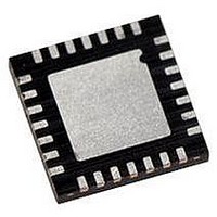
PIC18LF27J53-I/ML Microchip Technology, PIC18LF27J53-I/ML Datasheet - Page 443

PIC18LF27J53-I/ML
Manufacturer Part Number
PIC18LF27J53-I/ML
Description
IC PIC MCU 128KB FLASH 28QFN
Manufacturer
Microchip Technology
Series
PIC® XLP™ 18Fr
Datasheets
1.PIC18LF24J10-ISS.pdf
(32 pages)
2.PIC18F26J13-ISS.pdf
(496 pages)
3.PIC18F26J53-ISS.pdf
(586 pages)
4.PIC18F26J53-ISS.pdf
(12 pages)
Specifications of PIC18LF27J53-I/ML
Core Size
8-Bit
Program Memory Size
128KB (64K x 16)
Core Processor
PIC
Speed
48MHz
Connectivity
I²C, LIN, SPI, UART/USART, USB
Peripherals
Brown-out Detect/Reset, POR, PWM, WDT
Number Of I /o
22
Program Memory Type
FLASH
Ram Size
3.8K x 8
Voltage - Supply (vcc/vdd)
2 V ~ 2.75 V
Data Converters
A/D 10x10b/12b
Oscillator Type
Internal
Operating Temperature
-40°C ~ 85°C
Package / Case
*
Controller Family/series
PIC18
Cpu Speed
48MHz
Digital Ic Case Style
QFN
Supply Voltage Range
1.8V To 3.6V
Embedded Interface Type
I2C, SPI, USART
Rohs Compliant
Yes
Lead Free Status / RoHS Status
Lead free / RoHS Compliant
Eeprom Size
-
Lead Free Status / RoHS Status
Lead free / RoHS Compliant, Lead free / RoHS Compliant
Available stocks
Company
Part Number
Manufacturer
Quantity
Price
Company:
Part Number:
PIC18LF27J53-I/ML
Manufacturer:
ATMEL
Quantity:
101
- PIC18LF24J10-ISS PDF datasheet
- PIC18F26J13-ISS PDF datasheet #2
- PIC18F26J53-ISS PDF datasheet #3
- PIC18F26J53-ISS PDF datasheet #4
- Current page: 443 of 496
- Download datasheet (5Mb)
27.11.3
FIGURE 27-5:
TABLE 27-6:
2010 Microchip Technology Inc.
1A
1
2
3
4
Note 1:
Param.
CLKOUT
No.
OSC1
F
T
T
T
T
T
T
Instruction cycle period (T
except PLL. All specified values are based on characterization data for that particular oscillator type under
standard operating conditions with the device executing code. Exceeding these specified limits may result
in an unstable oscillator operation and/or higher than expected current consumption. All devices are tested
to operate at “min.” values with an external clock applied to the OSC1/CLKIN pin. When an external clock
input is used, the “max.” cycle time limit is “DC” (no clock) for all devices.
TIMING DIAGRAMS AND SPECIFICATIONS
Symbol
OSC
CY
OS
OS
OS
OS
OSC
L,
H
R,
F
EXTERNAL CLOCK TIMING REQUIREMENTS
EXTERNAL CLOCK TIMING (ALL MODES EXCEPT PLL)
External CLKIN
Frequency
Oscillator Frequency
External CLKIN Period
Oscillator Period
Instruction Cycle Time
External Clock in (OSC1)
High or Low Time
External Clock in (OSC1)
Rise or Fall Time
Q4
Characteristic
(1)
CY
(1)
) equals four times the input oscillator time base period for all configurations
Q1
1
(1)
(1)
(1)
Preliminary
62.5
15.6
62.5
62.5
Min
250
250
DC
DC
DC
DC
0.1
2.0
2.5
40
30
10
—
—
—
1
1
5
5
Q2
10,000
Max
200
250
250
200
0.5
7.5
16
64
20
20
50
—
—
—
—
—
—
—
—
4
4
4
2
3
PIC18(L)F2X/4XK22
Units
MHz
MHz
MHz
MHz
MHz
MHz
MHz
Q3
kHz
s
s
s
ns
ns
ns
ns
ns
ns
ns
ns
ns
ns
ns
ns
3
EC, ECIO Oscillator mode (low power)
EC, ECIO Oscillator mode (medium
power)
EC, ECIO Oscillator mode (high power)
RC Oscillator mode
XT Oscillator mode
HS Oscillator mode, V
HS Oscillator mode, V
LP Oscillator mode
EC, ECIO Oscillator mode (low power)
EC, ECIO Oscillator mode (medium
power)
EC, ECIO Oscillator mode (high power)
RC Oscillator mode
XT Oscillator mode
HS Oscillator mode
HS + PLL Oscillator mode,
LP Oscillator mode
T
XT Oscillator mode
LP Oscillator mode
HS Oscillator mode
XT Oscillator mode
LP Oscillator mode
HS Oscillator mode
CY
= 4/F
Q4
4
OSC
Conditions
4
DS41412D-page 443
DD
DD
Q1
> 2.7V
2.7V
Related parts for PIC18LF27J53-I/ML
Image
Part Number
Description
Manufacturer
Datasheet
Request
R

Part Number:
Description:
Manufacturer:
Microchip Technology Inc.
Datasheet:

Part Number:
Description:
Manufacturer:
Microchip Technology Inc.
Datasheet:

Part Number:
Description:
Manufacturer:
Microchip Technology Inc.
Datasheet:

Part Number:
Description:
Manufacturer:
Microchip Technology Inc.
Datasheet:

Part Number:
Description:
Manufacturer:
Microchip Technology Inc.
Datasheet:

Part Number:
Description:
Manufacturer:
Microchip Technology Inc.
Datasheet:

Part Number:
Description:
Manufacturer:
Microchip Technology Inc.
Datasheet:

Part Number:
Description:
Manufacturer:
Microchip Technology Inc.
Datasheet:


