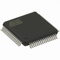
AT90CAN64-16AUR Atmel, AT90CAN64-16AUR Datasheet - Page 165

AT90CAN64-16AUR
Manufacturer Part Number
AT90CAN64-16AUR
Description
MCU AVR 64K FLASH 16MHZ 64TQFP
Manufacturer
Atmel
Series
AVR® 90CANr
Datasheet
1.AT90CAN32-16AUR.pdf
(428 pages)
Specifications of AT90CAN64-16AUR
Core Processor
AVR
Core Size
8-Bit
Speed
16MHz
Connectivity
CAN, EBI/EMI, I²C, SPI, UART/USART
Peripherals
Brown-out Detect/Reset, POR, PWM, WDT
Number Of I /o
53
Program Memory Size
64KB (64K x 8)
Program Memory Type
FLASH
Eeprom Size
2K x 8
Ram Size
4K x 8
Voltage - Supply (vcc/vdd)
2.7 V ~ 5.5 V
Data Converters
A/D 8x10b
Oscillator Type
Internal
Operating Temperature
-40°C ~ 85°C
Package / Case
64-TQFP, 64-VQFP
Data Bus Width
8 bit
Data Ram Size
4 KB
Mounting Style
SMD/SMT
Lead Free Status / RoHS Status
Lead free / RoHS Compliant
Available stocks
Company
Part Number
Manufacturer
Quantity
Price
- Current page: 165 of 428
- Download datasheet (6Mb)
15. Output Compare Modulator - OCM
15.1
15.2
7679H–CAN–08/08
Overview
Description
Many register and bit references in this section are written in general form.
The Output Compare Modulator (OCM) allows generation of waveforms modulated with a carrier
frequency. The modulator uses the outputs from the Output Compare Unit C of the 16-bit
Timer/Counter1 and the Output Compare Unit of the 8-bit Timer/Counter0. For more details
about these Timer/Counters see
on page 113
Figure 15-1. Output Compare Modulator, Block Diagram
When the modulator is enabled, the two output compare channels are modulated together as
shown in the block diagram
The Output Compare unit 1C and Output Compare unit 0A shares the PB7 port pin for output.
The outputs of the Output Compare units (OC1C and OC0A) overrides the normal PORTB7
Register when one of them is enabled (i.e., when COMnx1:0 is not equal to zero). When both
OC1C and OC0A are enabled at the same time, the modulator is automatically enabled.
When the modulator is enabled the type of modulation (logical AND or OR) can be selected by
the PORTB7 Register. Note that the DDRB7 controls the direction of the port independent of the
COMnx1:0 bit setting.
The functional equivalent schematic of the modulator is shown on
includes part of the Timer/Counter units and the port B pin 7 output driver circuit.
• A lower case “n” replaces the Timer/Counter number, in this case 0 and 1. However, when
• A lower case “x” replaces the Output Compare unit channel, in this case A or C. However,
using the register or bit defines in a program, the precise form must be used, i.e., TCNT0 for
accessing Timer/Counter0 counter value and so on.
when using the register or bit defines in a program, the precise form must be used, i.e.,
OCR0A for accessing Timer/Counter0 output compare channel A value and so on.
and
“8-bit Timer/Counter0 with PWM” on page
Timer/Counter 1
Timer/Counter 0
(Figure
“16-bit Timer/Counter (Timer/Counter1 and Timer/Counter3)”
15-1).
OC1C
OC0A
AT90CAN32/64/128
99.
Figure
OC0A / OC1C / PB7
15-2. The schematic
Pin
165
Related parts for AT90CAN64-16AUR
Image
Part Number
Description
Manufacturer
Datasheet
Request
R

Part Number:
Description:
Manufacturer:
Atmel Corporation
Datasheet:

Part Number:
Description:
Manufacturer:
Atmel Corporation
Datasheet:

Part Number:
Description:
IC MCU AVR 64K FLASH 64-TQFP
Manufacturer:
Atmel
Datasheet:

Part Number:
Description:
IC MCU AVR 64K FLASH 64-QFN
Manufacturer:
Atmel
Datasheet:

Part Number:
Description:
At90can128 8-bit Avr Microcontroller With 32k Bytes Of Isp Flash And Can Controller
Manufacturer:
ATMEL Corporation
Datasheet:

Part Number:
Description:
8-bit Microcontrollers - MCU 64 KB FLASH - 16MHz
Manufacturer:
Atmel

Part Number:
Description:
8-bit Microcontrollers - MCU Microcontroller
Manufacturer:
Atmel

Part Number:
Description:
DEV KIT FOR AVR/AVR32
Manufacturer:
Atmel
Datasheet:


