AT90CAN64-16AUR Atmel, AT90CAN64-16AUR Datasheet - Page 76
AT90CAN64-16AUR
Manufacturer Part Number
AT90CAN64-16AUR
Description
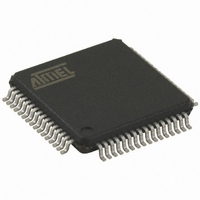
MCU AVR 64K FLASH 16MHZ 64TQFP
Manufacturer
Atmel
Series
AVR® 90CANr
Datasheet
1.AT90CAN32-16AUR.pdf
(428 pages)
Specifications of AT90CAN64-16AUR
Core Processor
AVR
Core Size
8-Bit
Speed
16MHz
Connectivity
CAN, EBI/EMI, I²C, SPI, UART/USART
Peripherals
Brown-out Detect/Reset, POR, PWM, WDT
Number Of I /o
53
Program Memory Size
64KB (64K x 8)
Program Memory Type
FLASH
Eeprom Size
2K x 8
Ram Size
4K x 8
Voltage - Supply (vcc/vdd)
2.7 V ~ 5.5 V
Data Converters
A/D 8x10b
Oscillator Type
Internal
Operating Temperature
-40°C ~ 85°C
Package / Case
64-TQFP, 64-VQFP
Data Bus Width
8 bit
Data Ram Size
4 KB
Mounting Style
SMD/SMT
Lead Free Status / RoHS Status
Lead free / RoHS Compliant
Available stocks
Company
Part Number
Manufacturer
Quantity
Price


9.3.3
76
AT90CAN32/64/128
Alternate Functions of Port B
The Port B pins with alternate functions are shown in
Table 9-6.
The alternate pin configuration is as follows:
• OC0A/OC1C, Bit 7
OC0A, Output Compare Match A output. The PB7 pin can serve as an external output for the
Timer/Counter0 Output Compare A. The pin has to be configured as an output (DDB7 set “one”)
to serve this function. The OC0A pin is also the output pin for the PWM mode timer function.
OC1C, Output Compare Match C output. The PB7 pin can serve as an external output for the
Timer/Counter1 Output Compare C. The pin has to be configured as an output (DDB7 set “one”)
to serve this function. The OC1C pin is also the output pin for the PWM mode timer function.
• OC1B, Bit 6
OC1B, Output Compare Match B output. The PB6 pin can serve as an external output for the
Timer/Counter1 Output Compare B. The pin has to be configured as an output (DDB6 set “one”)
to serve this function. The OC1B pin is also the output pin for the PWM mode timer function.
• OC1A, Bit 5
OC1A, Output Compare Match A output. The PB5 pin can serve as an external output for the
Timer/Counter1 Output Compare A. The pin has to be configured as an output (DDB5 set “one”)
to serve this function. The OC1A pin is also the output pin for the PWM mode timer function.
• OC2A, Bit 4
OC2A, Output Compare Match A output. The PB4 pin can serve as an external output for the
Timer/Counter2 Output Compare A. The pin has to be configured as an output (DDB4 set “one”)
to serve this function. The OC2A pin is also the output pin for the PWM mode timer function.
• MISO – Port B, Bit 3
MISO, Master Data input, Slave Data output pin for SPI channel. When the SPI is enabled as a
master, this pin is configured as an input regardless of the setting of DDB3. When the SPI is
enabled as a slave, the data direction of this pin is controlled by DDB3. When the pin is forced to
be an input, the pull-up can still be controlled by the PORTB3 bit.
• MOSI – Port B, Bit 2
Port Pin
PB7
PB6
PB5
PB4
PB3
PB2
PB1
PB0
Alternate Functions
OC0A/OC1C (Output Compare and PWM Output A for Timer/Counter0 or Output Compare
and PWM Output C for Timer/Counter1)
OC1B (Output Compare and PWM Output B for Timer/Counter1)
OC1A (Output Compare and PWM Output A for Timer/Counter1)
OC2A (Output Compare and PWM Output A for Timer/Counter2 )
MISO (SPI Bus Master Input/Slave Output)
MOSI (SPI Bus Master Output/Slave Input)
SCK (SPI Bus Serial Clock)
SS (SPI Slave Select input)
Port B Pins Alternate Functions
Table
9-6.
7679H–CAN–08/08
Related parts for AT90CAN64-16AUR
Image
Part Number
Description
Manufacturer
Datasheet
Request
R

Part Number:
Description:
Manufacturer:
Atmel Corporation
Datasheet:
Part Number:
Description:
Manufacturer:
Atmel Corporation
Datasheet:

Part Number:
Description:
IC MCU AVR 64K FLASH 64-TQFP
Manufacturer:
Atmel
Datasheet:

Part Number:
Description:
IC MCU AVR 64K FLASH 64-QFN
Manufacturer:
Atmel
Datasheet:

Part Number:
Description:
At90can128 8-bit Avr Microcontroller With 32k Bytes Of Isp Flash And Can Controller
Manufacturer:
ATMEL Corporation
Datasheet:

Part Number:
Description:
8-bit Microcontrollers - MCU 64 KB FLASH - 16MHz
Manufacturer:
Atmel
Part Number:
Description:
8-bit Microcontrollers - MCU Microcontroller
Manufacturer:
Atmel

Part Number:
Description:
DEV KIT FOR AVR/AVR32
Manufacturer:
Atmel
Datasheet: