PIC18LF47J53-I/ML Microchip Technology, PIC18LF47J53-I/ML Datasheet - Page 184
PIC18LF47J53-I/ML
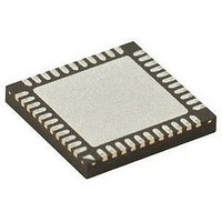
Manufacturer Part Number
PIC18LF47J53-I/ML
Description
IC PIC MCU 128KB FLASH 44QFN
Manufacturer
Microchip Technology
Series
PIC® XLP™ 18Fr
Datasheets
1.PIC18LF24J10-ISS.pdf
(32 pages)
2.PIC18F26J13-ISS.pdf
(496 pages)
3.PIC18F26J53-ISS.pdf
(586 pages)
4.PIC18F26J53-ISS.pdf
(12 pages)
Specifications of PIC18LF47J53-I/ML
Core Size
8-Bit
Program Memory Size
128KB (64K x 16)
Core Processor
PIC
Speed
48MHz
Connectivity
I²C, LIN, SPI, UART/USART, USB
Peripherals
Brown-out Detect/Reset, POR, PWM, WDT
Number Of I /o
34
Program Memory Type
FLASH
Ram Size
3.8K x 8
Voltage - Supply (vcc/vdd)
2 V ~ 2.75 V
Data Converters
A/D 13x10b/12b
Oscillator Type
Internal
Operating Temperature
-40°C ~ 85°C
Package / Case
*
Controller Family/series
PIC18
Cpu Speed
48MHz
Digital Ic Case Style
QFN
Supply Voltage Range
1.8V To 3.6V
Embedded Interface Type
I2C, SPI, USART
Rohs Compliant
Yes
Lead Free Status / RoHS Status
Lead free / RoHS Compliant
Eeprom Size
-
Lead Free Status / RoHS Status
Lead free / RoHS Compliant, Lead free / RoHS Compliant


PIC18(L)F2X/4XK22
14.3
Pulse-Width Modulation (PWM) is a scheme that
provides power to a load by switching quickly between
fully on and fully off states. The PWM signal resembles
a square wave where the high portion of the signal is
considered the on state and the low portion of the signal
is considered the off state. The high portion, also known
as the pulse width, can vary in time and is defined in
steps. A larger number of steps applied, which
lengthens the pulse width, also supplies more power to
the load. Lowering the number of steps applied, which
shortens the pulse width, supplies less power. The
PWM period is defined as the duration of one complete
cycle or the total amount of on and off time combined.
PWM resolution defines the maximum number of steps
that can be present in a single PWM period. A higher
resolution allows for more precise control of the pulse
width time and in turn the power that is applied to the
load.
The term duty cycle describes the proportion of the on
time to the off time and is expressed in percentages,
where 0% is fully off and 100% is fully on. A lower duty
cycle corresponds to less power applied and a higher
duty cycle corresponds to more power applied.
Figure 14-3
signal.
14.3.1
The standard PWM function described in this section is
available and identical for CCP and ECCP modules.
The standard PWM mode generates a Pulse-Width
modulation (PWM) signal on the CCPx pin with up to 10
bits of resolution. The period, duty cycle, and resolution
are controlled by the following registers:
• PRx registers
• TxCON registers
• CCPRxL registers
• CCPxCON registers
Figure 14-4
operation.
DS41412D-page 184
Note 1: The corresponding TRIS bit must be
2: Clearing the CCPxCON register will
PWM Overview
STANDARD PWM OPERATION
shows a simplified block diagram of PWM
cleared to enable the PWM output on the
CCPx pin.
relinquish control of the CCPx pin.
shows a typical waveform of the PWM
Preliminary
FIGURE 14-3:
FIGURE 14-4:
14.3.2
The following steps should be taken when configuring
the CCP module for standard PWM operation:
1.
2.
3.
4.
5.
Note 1:
Disable the CCPx pin output driver by setting the
associated TRIS bit.
Select the 8-bit TimerX resource, (Timer2,
Timer4 or Timer6) to be used for PWM genera-
tion by setting the CxTSEL<1:0> bits in the
CCPTMRSx register.
Load the PRx register for the selected TimerX
with the PWM period value.
Configure the CCP module for the PWM mode
by loading the CCPxCON register with the
appropriate values.
Load the CCPRxL register and the DCxB<1:0>
bits of the CCPxCON register, with the PWM
duty cycle value.
CCPRxH
Duty Cycle Registers
Comparator
2:
Pulse Width
CCPRxL
TMRx = 0
PRx
TMRx
Comparator
SETUP FOR PWM OPERATION
The 8-bit timer TMRx register is concatenated
with the 2-bit internal system clock (F
2 bits of the prescaler, to create the 10-bit time
base.
In PWM mode, CCPRxH is a read-only register.
(2)
Period
(Slave)
CCP PWM OUTPUT SIGNAL
(1)
SIMPLIFIED PWM BLOCK
DIAGRAM
Clear Timer,
toggle CCPx pin and
latch duty cycle
TMRx = CCPRxH:CCPxCON<5:4>
2010 Microchip Technology Inc.
CCPxCON<5:4>
(1)
TMRx = PRx
S
R
Q
TRIS
OSC
CCPx
), or
Related parts for PIC18LF47J53-I/ML
Image
Part Number
Description
Manufacturer
Datasheet
Request
R

Part Number:
Description:
Manufacturer:
Microchip Technology Inc.
Datasheet:
Part Number:
Description:
Manufacturer:
Microchip Technology Inc.
Datasheet:
Part Number:
Description:
Manufacturer:
Microchip Technology Inc.
Datasheet:
Part Number:
Description:
Manufacturer:
Microchip Technology Inc.
Datasheet:
Part Number:
Description:
Manufacturer:
Microchip Technology Inc.
Datasheet:
Part Number:
Description:
Manufacturer:
Microchip Technology Inc.
Datasheet:
Part Number:
Description:
Manufacturer:
Microchip Technology Inc.
Datasheet:
Part Number:
Description:
Manufacturer:
Microchip Technology Inc.
Datasheet: