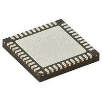
PIC18LF47J53-I/ML Microchip Technology, PIC18LF47J53-I/ML Datasheet - Page 298

PIC18LF47J53-I/ML
Manufacturer Part Number
PIC18LF47J53-I/ML
Description
IC PIC MCU 128KB FLASH 44QFN
Manufacturer
Microchip Technology
Series
PIC® XLP™ 18Fr
Datasheets
1.PIC18LF24J10-ISS.pdf
(32 pages)
2.PIC18F26J13-ISS.pdf
(496 pages)
3.PIC18F26J53-ISS.pdf
(586 pages)
4.PIC18F26J53-ISS.pdf
(12 pages)
Specifications of PIC18LF47J53-I/ML
Core Size
8-Bit
Program Memory Size
128KB (64K x 16)
Core Processor
PIC
Speed
48MHz
Connectivity
I²C, LIN, SPI, UART/USART, USB
Peripherals
Brown-out Detect/Reset, POR, PWM, WDT
Number Of I /o
34
Program Memory Type
FLASH
Ram Size
3.8K x 8
Voltage - Supply (vcc/vdd)
2 V ~ 2.75 V
Data Converters
A/D 13x10b/12b
Oscillator Type
Internal
Operating Temperature
-40°C ~ 85°C
Package / Case
*
Controller Family/series
PIC18
Cpu Speed
48MHz
Digital Ic Case Style
QFN
Supply Voltage Range
1.8V To 3.6V
Embedded Interface Type
I2C, SPI, USART
Rohs Compliant
Yes
Lead Free Status / RoHS Status
Lead free / RoHS Compliant
Eeprom Size
-
Lead Free Status / RoHS Status
Lead free / RoHS Compliant, Lead free / RoHS Compliant
- PIC18LF24J10-ISS PDF datasheet
- PIC18F26J13-ISS PDF datasheet #2
- PIC18F26J53-ISS PDF datasheet #3
- PIC18F26J53-ISS PDF datasheet #4
- Current page: 298 of 496
- Download datasheet (5Mb)
PIC18(L)F2X/4XK22
17.2.11
The following registers are used to control the
operation of the ADC.
REGISTER 17-1:
DS41412D-page 298
bit 7
Legend:
R = Readable bit
-n = Value at POR
bit 7
bit 6-2
bit 1
Note:
U-0
—
ADC REGISTER DEFINITIONS
Analog pin control is determined by the
ANSELx registers (see
Unimplemented: Read as ‘0’
CHS<4:0>: Analog Channel Select bits
00000 = AN0
00001 = AN1
00010 = AN2
00011 = AN3
00100 = AN4
00101 = AN5
00110 = AN6
00111 = AN7
01000 = AN8
01001 = AN9
01010 = AN10
01011 = AN11
01100 = AN12
01101 = AN13
01110 = AN14
01111 = AN15
10000 = AN16
10001 = AN17
10010 = AN18
10011 = AN19
10100 = AN20
10101 = AN21
10110 = AN22
10111 = AN23
11000 = AN24
11001 = AN25
11010 = AN26
11011 = AN27
11100 = Reserved
11101 = CTMU
11110 = DAC
11111 = FVR BUF2 (1.024V/2.048V/2.096V Volt Fixed Voltage Reference)
GO/DONE: A/D Conversion Status bit
1 = A/D conversion cycle in progress. Setting this bit starts an A/D conversion cycle.
0 = A/D conversion completed/not in progress
R/W-0
This bit is automatically cleared by hardware when the A/D conversion has completed.
ADCON0: A/D CONTROL REGISTER 0
(1)
(1)
(1)
W = Writable bit
‘1’ = Bit is set
(1)
(1)
(1)
(1)
(1)
(1)
(1)
(1)
R/W-0
Register
10-2)
CHS<4:0>
R/W-0
Preliminary
U = Unimplemented bit, read as ‘0’
‘0’ = Bit is cleared
R/W-0
R/W-0
2010 Microchip Technology Inc.
x = Bit is unknown
GO/DONE
(2)
R/W-0
ADON
R/W-0
bit 0
Related parts for PIC18LF47J53-I/ML
Image
Part Number
Description
Manufacturer
Datasheet
Request
R

Part Number:
Description:
Manufacturer:
Microchip Technology Inc.
Datasheet:

Part Number:
Description:
Manufacturer:
Microchip Technology Inc.
Datasheet:

Part Number:
Description:
Manufacturer:
Microchip Technology Inc.
Datasheet:

Part Number:
Description:
Manufacturer:
Microchip Technology Inc.
Datasheet:

Part Number:
Description:
Manufacturer:
Microchip Technology Inc.
Datasheet:

Part Number:
Description:
Manufacturer:
Microchip Technology Inc.
Datasheet:

Part Number:
Description:
Manufacturer:
Microchip Technology Inc.
Datasheet:

Part Number:
Description:
Manufacturer:
Microchip Technology Inc.
Datasheet:


