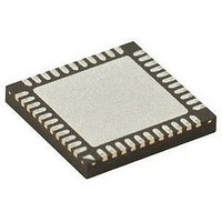
PIC18LF47J53-I/ML Microchip Technology, PIC18LF47J53-I/ML Datasheet - Page 21

PIC18LF47J53-I/ML
Manufacturer Part Number
PIC18LF47J53-I/ML
Description
IC PIC MCU 128KB FLASH 44QFN
Manufacturer
Microchip Technology
Series
PIC® XLP™ 18Fr
Datasheets
1.PIC18LF24J10-ISS.pdf
(32 pages)
2.PIC18F26J13-ISS.pdf
(496 pages)
3.PIC18F26J53-ISS.pdf
(586 pages)
4.PIC18F26J53-ISS.pdf
(12 pages)
Specifications of PIC18LF47J53-I/ML
Core Size
8-Bit
Program Memory Size
128KB (64K x 16)
Core Processor
PIC
Speed
48MHz
Connectivity
I²C, LIN, SPI, UART/USART, USB
Peripherals
Brown-out Detect/Reset, POR, PWM, WDT
Number Of I /o
34
Program Memory Type
FLASH
Ram Size
3.8K x 8
Voltage - Supply (vcc/vdd)
2 V ~ 2.75 V
Data Converters
A/D 13x10b/12b
Oscillator Type
Internal
Operating Temperature
-40°C ~ 85°C
Package / Case
*
Controller Family/series
PIC18
Cpu Speed
48MHz
Digital Ic Case Style
QFN
Supply Voltage Range
1.8V To 3.6V
Embedded Interface Type
I2C, SPI, USART
Rohs Compliant
Yes
Lead Free Status / RoHS Status
Lead free / RoHS Compliant
Eeprom Size
-
Lead Free Status / RoHS Status
Lead free / RoHS Compliant, Lead free / RoHS Compliant
- PIC18LF24J10-ISS PDF datasheet
- PIC18F26J13-ISS PDF datasheet #2
- PIC18F26J53-ISS PDF datasheet #3
- PIC18F26J53-ISS PDF datasheet #4
- Current page: 21 of 496
- Download datasheet (5Mb)
TABLE 1-2:
TABLE 1-3:
2010 Microchip Technology Inc.
Legend:
Note 1:
Legend:
PDIP
Note
PDIP,
SOIC
8, 19
Pin Number
2
3
4
5
6
20
2:
TQFP
1: Default pin assignment for P2B, T3CKI, CCP3/P3A and CCP2/P2A when Configuration bits PB2MX, T3CMX, CCP3MX
2: Alternate pin assignment for P2B, T3CKI, CCP3/P3A and CCP2/P2A when Configuration bits PB2MX, T3CMX,
19
20
21
22
23
UQFN
Pin Number
QFN,
5, 16
17
TTL = TTL compatible input CMOS = CMOS compatible input or output; ST = Schmitt Trigger input with CMOS levels;
I = Input; O = Output; P = Power.
Default pin assignment for P2B, T3CKI, CCP3 and CCP2 when Configuration bits PB2MX, T3CMX, CCP3MX and
CCP2MX are set.
Alternate pin assignment for P2B, T3CKI, CCP3 and CCP2 when Configuration bits PB2MX, T3CMX, CCP3MX and
CCP2MX are clear.
TTL = TTL compatible input CMOS = CMOS compatible input or output; ST = Schmitt Trigger input with CMOS levels;
I = Input; O = Output; P = Power.
and CCP2MX are set.
CCP3MX and CCP2MX are clear.
QFN
19
20
21
22
23
PIC18(L)F2XK22 PINOUT I/O DESCRIPTIONS (CONTINUED)
PIC18(L)F4XK22 PINOUT I/O DESCRIPTIONS
UQFN
17
18
19
20
21
Pin Name
V
V
RA0/C12IN0-/AN0
RA1/C12IN1-/AN1
RA2/C2IN+/AN2/DACOUT/V
RA3/C1IN+/AN3/V
RA4/C1OUT/SRQ/T0CKI
DD
SS
Pin Name
DACOUT
C12IN0-
C12IN1-
C1OUT
C2IN+
C1IN+
T0CKI
V
V
SRQ
RA0
AN0
RA1
AN1
RA2
AN2
RA3
AN3
RA4
REF
REF
+
-
REF
Preliminary
Type
+
Pin
P
P
Type
REF
Pin
Buffer
I/O
I/O
I/O
I/O
I/O
O
O
O
Type
I
I
I
I
I
I
I
I
I
I
I
—
—
-
Analog Comparators C1 and C2 inverting input.
Analog Analog input 0.
Analog Comparators C1 and C2 inverting input.
Analog Analog input 1.
Analog Comparator C2 non-inverting input.
Analog Analog input 2.
Analog DAC Reference output.
Analog A/D reference voltage (low) input.
Analog Comparator C1 non-inverting input.
Analog Analog input 3.
Analog A/D reference voltage (high) input.
Buffer
CMOS Comparator C1 output.
Type
TTL
TTL
TTL
TTL
TTL
PIC18(L)F2X/4XK22
Positive supply for logic and I/O pins.
Ground reference for logic and I/O pins.
ST
ST
Digital I/O.
Digital I/O.
Digital I/O.
Digital I/O.
Digital I/O.
SR Latch Q output.
Timer0 external clock input.
Description
Description
DS41412D-page 21
Related parts for PIC18LF47J53-I/ML
Image
Part Number
Description
Manufacturer
Datasheet
Request
R

Part Number:
Description:
Manufacturer:
Microchip Technology Inc.
Datasheet:

Part Number:
Description:
Manufacturer:
Microchip Technology Inc.
Datasheet:

Part Number:
Description:
Manufacturer:
Microchip Technology Inc.
Datasheet:

Part Number:
Description:
Manufacturer:
Microchip Technology Inc.
Datasheet:

Part Number:
Description:
Manufacturer:
Microchip Technology Inc.
Datasheet:

Part Number:
Description:
Manufacturer:
Microchip Technology Inc.
Datasheet:

Part Number:
Description:
Manufacturer:
Microchip Technology Inc.
Datasheet:

Part Number:
Description:
Manufacturer:
Microchip Technology Inc.
Datasheet:


