PIC18LF47J53-I/ML Microchip Technology, PIC18LF47J53-I/ML Datasheet - Page 191
PIC18LF47J53-I/ML
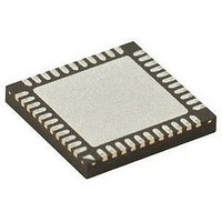
Manufacturer Part Number
PIC18LF47J53-I/ML
Description
IC PIC MCU 128KB FLASH 44QFN
Manufacturer
Microchip Technology
Series
PIC® XLP™ 18Fr
Datasheets
1.PIC18LF24J10-ISS.pdf
(32 pages)
2.PIC18F26J13-ISS.pdf
(496 pages)
3.PIC18F26J53-ISS.pdf
(586 pages)
4.PIC18F26J53-ISS.pdf
(12 pages)
Specifications of PIC18LF47J53-I/ML
Core Size
8-Bit
Program Memory Size
128KB (64K x 16)
Core Processor
PIC
Speed
48MHz
Connectivity
I²C, LIN, SPI, UART/USART, USB
Peripherals
Brown-out Detect/Reset, POR, PWM, WDT
Number Of I /o
34
Program Memory Type
FLASH
Ram Size
3.8K x 8
Voltage - Supply (vcc/vdd)
2 V ~ 2.75 V
Data Converters
A/D 13x10b/12b
Oscillator Type
Internal
Operating Temperature
-40°C ~ 85°C
Package / Case
*
Controller Family/series
PIC18
Cpu Speed
48MHz
Digital Ic Case Style
QFN
Supply Voltage Range
1.8V To 3.6V
Embedded Interface Type
I2C, SPI, USART
Rohs Compliant
Yes
Lead Free Status / RoHS Status
Lead free / RoHS Compliant
Eeprom Size
-
Lead Free Status / RoHS Status
Lead free / RoHS Compliant, Lead free / RoHS Compliant


14.4.1
In Half-Bridge mode, two pins are used as outputs to
drive push-pull loads. The PWM output signal is output
on the CCPx/PxA pin, while the complementary PWM
output signal is output on the PxB pin (see
This mode can be used for Half-Bridge applications, as
shown in
where four power switches are being modulated with
two PWM signals.
In Half-Bridge mode, the programmable dead-band delay
can be used to prevent shoot-through current in Half-
Bridge power devices. The value of the PDC<6:0> bits of
the PWMxCON register sets the number of instruction
cycles before the output is driven active. If the value is
greater than the duty cycle, the corresponding output
remains
Section 14.4.5 “Programmable Dead-Band Delay
Mode”
operations.
FIGURE 14-9:
2010 Microchip Technology Inc.
Standard Half-Bridge Circuit (“Push-Pull”)
Half-Bridge Output Driving a Full-Bridge Circuit
for more details of the dead-band delay
Figure
inactive
HALF-BRIDGE MODE
14-9, or for Full-Bridge applications,
during
EXAMPLE OF HALF-BRIDGE APPLICATIONS
the
PxA
PxB
entire
Figure
cycle.
PxA
PxB
FET
Driver
FET
Driver
14-9).
See
Preliminary
FET
Driver
FET
Driver
Since the PxA and PxB outputs are multiplexed with the
PORT data latches, the associated TRIS bits must be
cleared to configure PxA and PxB as outputs.
FIGURE 14-8:
PxA
PxB
td = Dead-Band Delay
Note 1: At this time, the TMRx register is equal to the
Load
PIC18(L)F2X/4XK22
V+
(2)
(2)
2: Output signals are shown as active-high.
(1)
td
PRx register.
Pulse Width
Load
Period
td
FET
Driver
FET
Driver
EXAMPLE OF HALF-
BRIDGE PWM OUTPUT
+
-
+
-
(1)
DS41412D-page 191
Period
(1)
Related parts for PIC18LF47J53-I/ML
Image
Part Number
Description
Manufacturer
Datasheet
Request
R

Part Number:
Description:
Manufacturer:
Microchip Technology Inc.
Datasheet:
Part Number:
Description:
Manufacturer:
Microchip Technology Inc.
Datasheet:
Part Number:
Description:
Manufacturer:
Microchip Technology Inc.
Datasheet:
Part Number:
Description:
Manufacturer:
Microchip Technology Inc.
Datasheet:
Part Number:
Description:
Manufacturer:
Microchip Technology Inc.
Datasheet:
Part Number:
Description:
Manufacturer:
Microchip Technology Inc.
Datasheet:
Part Number:
Description:
Manufacturer:
Microchip Technology Inc.
Datasheet:
Part Number:
Description:
Manufacturer:
Microchip Technology Inc.
Datasheet: