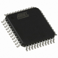
AT89C51RE2-RLTUM Atmel, AT89C51RE2-RLTUM Datasheet - Page 28

AT89C51RE2-RLTUM
Manufacturer Part Number
AT89C51RE2-RLTUM
Description
MCU 8051 128K FLASH 44-VQFP
Manufacturer
Atmel
Series
89Cr
Datasheet
1.AT89C51RE2-SLSUM.pdf
(187 pages)
Specifications of AT89C51RE2-RLTUM
Core Processor
8051
Core Size
8-Bit
Speed
60MHz
Connectivity
I²C, SPI, UART/USART
Peripherals
POR, PWM, WDT
Number Of I /o
34
Program Memory Size
128KB (128K x 8)
Program Memory Type
FLASH
Ram Size
8K x 8
Voltage - Supply (vcc/vdd)
2.7 V ~ 5.5 V
Oscillator Type
External
Operating Temperature
-40°C ~ 85°C
Package / Case
44-TQFP, 44-VQFP
Processor Series
AT89x
Core
8051
Data Bus Width
8 bit
Data Ram Size
8 KB
Interface Type
UART, SPI
Maximum Clock Frequency
60 MHz
Number Of Programmable I/os
34
Number Of Timers
3
Operating Supply Voltage
2.7 V to 5.5 V
Maximum Operating Temperature
+ 85 C
Mounting Style
SMD/SMT
3rd Party Development Tools
PK51, CA51, A51, ULINK2
Development Tools By Supplier
AT89OCD-01
Minimum Operating Temperature
- 40 C
Height
1.45 mm
Length
10.1 mm
Supply Voltage (max)
5.5 V
Supply Voltage (min)
2.7 V
Width
10.1 mm
For Use With
AT89STK-11 - KIT STARTER FOR AT89C51RX2
Lead Free Status / RoHS Status
Lead free / RoHS Compliant
Eeprom Size
-
Data Converters
-
Lead Free Status / Rohs Status
Details
Available stocks
Company
Part Number
Manufacturer
Quantity
Price
Company:
Part Number:
AT89C51RE2-RLTUM
Manufacturer:
MSC
Quantity:
1 560
Physical memory
organisation
On-Chip Flash
memory
28
AT89C51RE2
Figure 9. Physical memory organisation
The AT89C51RE2 implements up to 128K bytes of on-chip program/code memory. Figure 9 and
Figure 10 shows the partitioning of internal and external program/code memory spaces accord-
ing to EA value.
The memory partitioning of the 8051 core microcontroller is typical a Harvard architecture where
program and data areas are held in separate memory areas. The program and data memory
areas use the same physical address range from 0000H-FFFFH and a 8 bit instruction
code/data format.
To access more than 64kBytes of code memory, without modifications of the MCU core, and
development tools, the bank switching method is used.
The internal program memory is expanded to 128kByte in the ´Expanded Configuration’, the
data memory remains in the ´Normal Configuration´. The program memory is split into four 32
kByte banks (named Bank 0-2). The MCU core still addresses up to 64kBytes where the upper
32Kbytes can be selected between 3 32K bytes bank of on-chip flash memory. The lower 32K
bank is used as common area for interrupt subroutines, bank switching and functions calls
between banks.
The AT89C51RE2 also implements an extra upper 32K bank (Bank3) that allows external code
execution.
Fuse Configuration Byte(1 byte)
Hardware Security (1 byte)
Extra Row FM0 (128 bytes)
Column Latches (128 bytes)
1FFFFh
00000h
FCB
HSB
Flash memory
128K bytes
user space
FM0
4K bytes
ROM
RM0
7663E–8051–10/08


