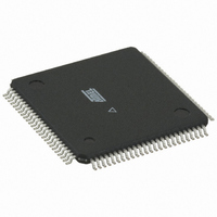
ATMEGA1280V-8AUR Atmel, ATMEGA1280V-8AUR Datasheet - Page 339

ATMEGA1280V-8AUR
Manufacturer Part Number
ATMEGA1280V-8AUR
Description
MCU AVR 128K FLASH 8MHZ 100TQFP
Manufacturer
Atmel
Series
AVR® ATmegar
Specifications of ATMEGA1280V-8AUR
Core Processor
AVR
Core Size
8-Bit
Speed
8MHz
Connectivity
EBI/EMI, I²C, SPI, UART/USART
Peripherals
Brown-out Detect/Reset, POR, PWM, WDT
Number Of I /o
86
Program Memory Size
128KB (64K x 16)
Program Memory Type
FLASH
Eeprom Size
4K x 8
Ram Size
8K x 8
Voltage - Supply (vcc/vdd)
1.8 V ~ 5.5 V
Data Converters
A/D 16x10b
Oscillator Type
Internal
Operating Temperature
-40°C ~ 85°C
Package / Case
100-TQFP, 100-VQFP
For Use With
ATSTK600-TQFP100 - STK600 SOCKET/ADAPTER 100-TQFPATSTK503 - STARTER KIT AVR EXP MODULE 100P
Lead Free Status / RoHS Status
Lead free / RoHS Compliant
Available stocks
Company
Part Number
Manufacturer
Quantity
Price
- Current page: 339 of 444
- Download datasheet (10Mb)
29.6.1
2549M–AVR–09/10
Signal Names
In this section, some pins of the ATmega640/1280/1281/2560/2561 are referenced by signal
names describing their functionality during parallel programming, see
9. Pins not described in the following table are referenced by pin names.
The XA1/XA0 pins determine the action executed when the XTAL1 pin is given a positive pulse.
The bit coding is shown in
When pulsing WR or OE, the command loaded determines the action executed. The different
commands are shown in
Figure 29-1. Parallel Programming
Note:
Table 29-9.
Programming Mode
Signal Name in
RDY/BSY
Unused Pins should be left floating.
PAGEL
DATA
BS1
XA0
XA1
BS2
WR
OE
Pin Name Mapping
Table 29-13 on page
RDY/BSY
Pin Name
Table 29-12 on page
PAGEL
PB7-0
+12V
PD1
PD2
PD3
PD4
PD5
PD6
PD7
BS1
XA0
XA1
BS2
PA0
WR
OE
ATmega640/1280/1281/2560/2561
(Note:)
I/O
I/O
PD1
PD2
PD3
PD4
PD5
PD6
PD7
RESET
XTAL1
GND
O
PA0
I
I
I
I
I
I
I
Program Memory and EEPROM data Page Load.
Bi-directional Data bus (Output when OE is low).
Function
0: Device is busy programming, 1: Device is ready for
new command.
Output Enable (Active low).
Write Pulse (Active low).
Byte Select 1.
XTAL Action Bit 0
XTAL Action Bit 1
Byte Select 2.
340.
340.
PB7 - PB0
AVCC
VCC
+5V
+5V
DATA
Figure 29-1
and
Table 29-
339
Related parts for ATMEGA1280V-8AUR
Image
Part Number
Description
Manufacturer
Datasheet
Request
R

Part Number:
Description:
Manufacturer:
Atmel Corporation
Datasheet:

Part Number:
Description:
IC MCU AVR 128K FLASH 100-CBGA
Manufacturer:
Atmel
Datasheet:

Part Number:
Description:
IC MCU AVR 128K FLASH 100-TQFP
Manufacturer:
Atmel
Datasheet:

Part Number:
Description:
MCU AVR 128K FLASH 16MHZ 100TQFP
Manufacturer:
Atmel
Datasheet:

Part Number:
Description:
MCU AVR 128K FLASH 16MHZ 100CBGA
Manufacturer:
Atmel
Datasheet:

Part Number:
Description:
Manufacturer:
ATMEL Corporation
Datasheet:

Part Number:
Description:
Microcontroller with 128K bytes In-system programmable flash, 8 MHz, power supply =2.7 - 5.5V
Manufacturer:
ATMEL Corporation
Datasheet:

Part Number:
Description:
IC AVR MCU 128K 16MHZ 5V 64TQFP
Manufacturer:
Atmel
Datasheet:

Part Number:
Description:
IC AVR MCU 128K 16MHZ 5V 64-QFN
Manufacturer:
Atmel
Datasheet:

Part Number:
Description:
IC AVR MCU 128K 16MHZ COM 64-QFN
Manufacturer:
Atmel
Datasheet:

Part Number:
Description:
IC AVR MCU 128K 16MHZ 64-TQFP
Manufacturer:
Atmel
Datasheet:


