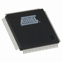
AT91SAM7X128B-AU Atmel, AT91SAM7X128B-AU Datasheet - Page 13

AT91SAM7X128B-AU
Manufacturer Part Number
AT91SAM7X128B-AU
Description
IC MCU 128KB FLASH 100LQFP
Manufacturer
Atmel
Series
AT91SAMr
Specifications of AT91SAM7X128B-AU
Core Processor
ARM7
Core Size
16/32-Bit
Speed
55MHz
Connectivity
CAN, Ethernet, I²C, SPI, SSC, UART/USART, USB
Peripherals
Brown-out Detect/Reset, DMA, POR, PWM, WDT
Number Of I /o
62
Program Memory Size
128KB (128K x 8)
Program Memory Type
FLASH
Ram Size
32K x 8
Voltage - Supply (vcc/vdd)
1.65 V ~ 1.95 V
Data Converters
A/D 8x10b
Oscillator Type
Internal
Operating Temperature
-40°C ~ 85°C
Package / Case
100-LQFP
Processor Series
AT91SAMx
Core
ARM7TDMI
Data Bus Width
32 bit
Data Ram Size
32 KB
Interface Type
JTAG, SPI, UART
Maximum Clock Frequency
55 MHz
Number Of Timers
1
Maximum Operating Temperature
+ 85 C
Mounting Style
SMD/SMT
3rd Party Development Tools
JTRACE-ARM-2M, KSK-AT91SAM7X-PL, MDK-ARM, RL-ARM, ULINK2
Development Tools By Supplier
AT91SAM-ICE, AT91-ISP, AT91SAM7X-EK
Minimum Operating Temperature
- 40 C
On-chip Adc
10 bit, 8 Channel
Controller Family/series
AT91SAM7xxxxx
No. Of I/o's
62
Ram Memory Size
32KB
Cpu Speed
55MHz
No. Of Timers
1
Rohs Compliant
Yes
Cpu Family
91S
Device Core
ARM7TDMI
Device Core Size
32b
Frequency (max)
55MHz
Total Internal Ram Size
32KB
# I/os (max)
62
Number Of Timers - General Purpose
3
Operating Supply Voltage (typ)
1.8/3.3V
Operating Supply Voltage (max)
1.95/3.6V
Operating Supply Voltage (min)
1.65/3V
Instruction Set Architecture
RISC
Operating Temp Range
-40C to 85C
Operating Temperature Classification
Industrial
Mounting
Surface Mount
Pin Count
100
Package Type
LQFP
Lead Free Status / RoHS Status
Lead free / RoHS Compliant
Eeprom Size
-
Lead Free Status / Rohs Status
Lead free / RoHS Compliant
Available stocks
Company
Part Number
Manufacturer
Quantity
Price
Company:
Part Number:
AT91SAM7X128B-AU
Manufacturer:
Atmel
Quantity:
1 929
Part Number:
AT91SAM7X128B-AU
Manufacturer:
ATMEL/爱特梅尔
Quantity:
20 000
6. I/O Lines Considerations
6.1
6.2
6.3
6.4
6120FS–ATARM–17-Feb-09
JTAG Port Pins
Test Pin
Reset Pin
ERASE Pin
TMS, TDI and TCK are schmitt trigger inputs and are not 5-V tolerant. TMS, TDI and TCK do not
integrate a pull-up resistor.
TDO is an output, driven at up to VDDIO, and has no pull-up resistor.
The JTAGSEL pin is used to select the JTAG boundary scan when asserted at a high level. The
JTAGSEL pin integrates a permanent pull-down resistor of about 15 kΩ to GND.
To eliminate any risk of spuriously entering the JTAG boundary scan mode due to noise on
JTAGSEL, it should be tied externally to GND if boundary scan is not used, or pulled down with
an external low-value resistor (such as 1 kΩ) .
T h e T S T p i n i s u s e d f o r m a n u f a c t u r i n g t e s t o r f a s t p r o g r a m m i n g m o d e o f t h e
AT91SAM7X512/256/128 when asserted high. The TST pin integrates a permanent pull-down
resistor of about 15 kΩ to GND.
To eliminate any risk of entering the test mode due to noise on the TST pin, it should be tied to
GND if the FFPI is not used, or pulled down with an external low-value resistor (such as 1 kΩ)
To enter fast programming mode, the TST pin and the PA0 and PA1 pins should be tied high
and PA2 tied to low.
Driving the TST pin at a high level while PA0 or PA1 is driven at 0 leads to unpredictable results.
The NRST pin is bidirectional with an open drain output buffer. It is handled by the on-chip reset
controller and can be driven low to provide a reset signal to the external components or asserted
low externally to reset the microcontroller. There is no constraint on the length of the reset pulse,
and the reset controller can guarantee a minimum pulse length. This allows connection of a sim-
ple push-button on the NRST pin as system user reset, and the use of the signal NRST to reset
all the components of the system.
The NRST pin integrates a permanent pull-up resistor to VDDIO.
The ERASE pin is used to re-initialize the Flash content and some of its NVM bits. It integrates a
permanent pull-down resistor of about 15 kΩ to GND.
To eliminate any risk of erasing the Flash due to noise on the ERASE pin, it shoul be tied exter-
nally to GND, which prevents erasing the Flash from the applicatiion, or pulled down with an
external low-value resistor (such as 1 kΩ) .
This pin is debounced by the RC oscillator to improve the glitch tolerance. When the pin is tied to
high during less than 100 ms, ERASE pin is not taken into account. The pin must be tied high
during more than 220 ms to perform the re-initialization of the Flash.
AT91SAM7X512/256/128 Preliminary Summary
13


