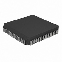
PIC17LC756A-08I/L Microchip Technology, PIC17LC756A-08I/L Datasheet - Page 14

PIC17LC756A-08I/L
Manufacturer Part Number
PIC17LC756A-08I/L
Description
IC MCU OTP 16KX16 A/D 68PLCC
Manufacturer
Microchip Technology
Series
PIC® 17Cr
Specifications of PIC17LC756A-08I/L
Core Processor
PIC
Core Size
8-Bit
Speed
8MHz
Connectivity
I²C, SPI, UART/USART
Peripherals
Brown-out Detect/Reset, POR, PWM, WDT
Number Of I /o
50
Program Memory Size
32KB (16K x 16)
Program Memory Type
OTP
Ram Size
902 x 8
Voltage - Supply (vcc/vdd)
3 V ~ 5.5 V
Data Converters
A/D 12x10b
Oscillator Type
External
Operating Temperature
-40°C ~ 85°C
Package / Case
68-PLCC
Processor Series
PIC17LC
Core
PIC
Data Bus Width
8 bit
Data Ram Size
902 B
Interface Type
I2C, MSSP, RS- 232, SCI, SPI, USART
Maximum Clock Frequency
8 MHz
Number Of Programmable I/os
50
Number Of Timers
8
Operating Supply Voltage
3 V to 5.5 V
Maximum Operating Temperature
+ 85 C
Mounting Style
SMD/SMT
Minimum Operating Temperature
- 40 C
On-chip Adc
12 bit
Lead Free Status / RoHS Status
Lead free / RoHS Compliant
Eeprom Size
-
Lead Free Status / Rohs Status
Details
Available stocks
Company
Part Number
Manufacturer
Quantity
Price
Company:
Part Number:
PIC17LC756A-08I/L
Manufacturer:
MICROCHIP
Quantity:
3 000
Company:
Part Number:
PIC17LC756A-08I/L
Manufacturer:
Microchip Technology
Quantity:
10 000
- Current page: 14 of 304
- Download datasheet (6Mb)
PIC17C7XX
TABLE 3-1:
DS30289B-page 14
OSC1/CLKIN
OSC2/CLKOUT
MCLR/V
RA0/INT
RA1/T0CKI
RA2/SS/SCL
RA3/SDI/SDA
RA4/RX1/DT1
RA5/TX1/CK1
RB0/CAP1
RB1/CAP2
RB2/PWM1
RB3/PWM2
RB4/TCLK12
RB5/TCLK3
RB6/SCK
RB7/SDO
Legend: I = Input only;
Note 1: The output is only available by the peripheral operation.
Name
2: Open drain input/output pin. Pin forced to input upon any device RESET.
PP
P = Power;
PINOUT DESCRIPTIONS
DIP
No.
47
48
15
56
41
42
43
40
39
55
54
50
53
52
51
44
45
PIC17C75X
O = Output only;
— = Not Used;
PLCC
No.
50
51
16
60
44
45
46
43
42
59
58
54
57
56
55
47
48
TQFP
No.
39
40
48
33
34
35
32
31
47
46
42
45
44
43
36
37
7
PLCC
No.
PIC17C76X
62
63
20
72
56
57
58
51
50
71
70
66
69
68
67
59
60
I/O = Input/Output;
TTL = TTL input;
QFP
No.
49
50
58
43
44
45
38
37
57
56
52
55
54
53
46
47
9
I/O/P
Type
I/O
I/O
I/O
I/O
I/O
I/O
I/O
I/O
I/O
I/O
I/O
I/O
I/P
O
I
I
I
(2)
(2)
(1)
(1)
Buffer
Type
ST
ST
ST
ST
ST
ST
ST
ST
ST
ST
ST
ST
ST
ST
ST
ST
—
ST = Schmitt Trigger input
Oscillator input in Crystal/Resonator or RC Oscillator
mode. External clock input in External Clock mode.
Oscillator output. Connects to crystal or resonator in
Crystal Oscillator mode. In RC Oscillator or External
Clock modes, OSC2 pin outputs CLKOUT which has
one fourth the frequency (F
denotes the instruction cycle rate.
Master clear (RESET) input or Programming Voltage
(V
device.
PORTA pins have individual differentiations that are
listed in the following descriptions:
PORTB is a bi-directional I/O Port with software
configurable weak pull-ups.
PP
) input. This is the active low RESET input to the
RA0 can also be selected as an external inter-
rupt input. Interrupt can be configured to be on
positive or negative edge. Input only pin.
RA1 can also be selected as an external inter-
rupt input and the interrupt can be configured to
be on positive or negative edge. RA1 can also
be selected to be the clock input to the Timer0
timer/counter. Input only pin.
RA2 can also be used as the slave select input
for the SPI or the clock input for the I
High voltage, high current, open drain port pin.
RA3 can also be used as the data input for the
SPI or the data for the I
High voltage, high current, open drain port pin.
RA4 can also be selected as the USART1 (SCI)
Asynchronous Receive or USART1 (SCI)
Synchronous Data.
Output available from USART only.
RA5 can also be selected as the USART1 (SCI)
Asynchronous Transmit or USART1 (SCI)
Synchronous Clock.
Output available from USART only.
RB0 can also be the Capture1 input pin.
RB1 can also be the Capture2 input pin.
RB2 can also be the PWM1 output pin.
RB3 can also be the PWM2 output pin.
RB4 can also be the external clock input to
Timer1 and Timer2.
RB5 can also be the external clock input to
Timer3.
RB6 can also be used as the master/slave clock
for the SPI.
RB7 can also be used as the data output for the
SPI.
Description
2000 Microchip Technology Inc.
OSC
2
C bus.
/4) of OSC1 and
2
C bus.
Related parts for PIC17LC756A-08I/L
Image
Part Number
Description
Manufacturer
Datasheet
Request
R

Part Number:
Description:
MICRO CTRL 16K LOW PWR 68PLCC
Manufacturer:
Microchip Technology
Datasheet:

Part Number:
Description:
MICRO CTRL 16K LOW PWR 64SDIP
Manufacturer:
Microchip Technology
Datasheet:

Part Number:
Description:
MICRO CTRL 16K LOW PWR 64SDIP
Manufacturer:
Microchip Technology
Datasheet:

Part Number:
Description:
MICRO CTRL 16K LOW PWR 68PLCC
Manufacturer:
Microchip Technology
Datasheet:

Part Number:
Description:
Manufacturer:
Microchip Technology Inc.
Datasheet:

Part Number:
Description:
Manufacturer:
Microchip Technology Inc.
Datasheet:

Part Number:
Description:
Manufacturer:
Microchip Technology Inc.
Datasheet:

Part Number:
Description:
Manufacturer:
Microchip Technology Inc.
Datasheet:

Part Number:
Description:
Manufacturer:
Microchip Technology Inc.
Datasheet:

Part Number:
Description:
Manufacturer:
Microchip Technology Inc.
Datasheet:

Part Number:
Description:
Manufacturer:
Microchip Technology Inc.
Datasheet:


