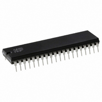
P87C52X2FN,112 NXP Semiconductors, P87C52X2FN,112 Datasheet - Page 31

P87C52X2FN,112
Manufacturer Part Number
P87C52X2FN,112
Description
IC 80C51 MCU 256 RAM 40DIP
Manufacturer
NXP Semiconductors
Series
87Cr
Datasheet
1.P87C52X2BN112.pdf
(62 pages)
Specifications of P87C52X2FN,112
Core Processor
8051
Core Size
8-Bit
Speed
33MHz
Connectivity
EBI/EMI, UART/USART
Peripherals
POR
Number Of I /o
32
Program Memory Size
8KB (8K x 8)
Program Memory Type
OTP
Ram Size
256 x 8
Voltage - Supply (vcc/vdd)
2.7 V ~ 5.5 V
Oscillator Type
Internal
Operating Temperature
-40°C ~ 85°C
Package / Case
40-DIP (0.600", 15.24mm)
Processor Series
P87C5x
Core
80C51
Data Bus Width
8 bit
Data Ram Size
256 B
Interface Type
UART
Maximum Clock Frequency
33 MHz
Number Of Programmable I/os
32
Number Of Timers
3
Operating Supply Voltage
2.7 V to 5.5 V
Maximum Operating Temperature
+ 85 C
Mounting Style
SMD/SMT
3rd Party Development Tools
PK51, CA51, A51, ULINK2
Minimum Operating Temperature
- 40 C
Package
40PDIP
Device Core
80C51
Family Name
87C
Maximum Speed
33 MHz
Lead Free Status / RoHS Status
Lead free / RoHS Compliant
Eeprom Size
-
Data Converters
-
Lead Free Status / Rohs Status
Details
Other names
935269602112
P87C52X2FN
P87C52X2FN
P87C52X2FN
P87C52X2FN
Philips Semiconductors
2003 Jan 24
NOTES:
*SMOD0 is located at PCON.6.
**f
80C51 8-bit microcontroller family
4K/8K/16K/32K ROM/OTP, low voltage (2.7 to 5.5 V),
low power, high speed (30/33 MHz)
SCON Address = 98H
OSC
Symbol
FE
SM0
SM1
SM2
REN
TB8
RB8
Tl
Rl
= oscillator frequency
Bit Addressable
Position
SCON.7
SCON.7
SCON.6
SCON.5
SCON.4
SCON.3
SCON.2
SCON.1
SCON.0
(SMOD0 = 0/1)*
SM0/FE
7
Framing Error bit. This bit is set by the receiver when an invalid stop bit is detected. The FE bit is not
cleared by valid frames but should be cleared by software. The SMOD0 bit must be set to enable
access to the FE bit.*
Serial Port Mode Bit 0, (SMOD0 must = 0 to access bit SM0)
Serial Port Mode Bit 1
Enables the Automatic Address Recognition feature in Modes 2 or 3. If SM2 = 1 then Rl will not be set
unless the received 9th data bit (RB8) is 1, indicating an address, and the received byte is a Given or
Broadcast Address. In Mode 1, if SM2 = 1 then Rl will not be activated unless a valid stop bit was
received, and the received byte is a Given or Broadcast Address. In Mode 0, SM2 should be 0.
Enables serial reception. Set by software to enable reception. Clear by software to disable reception.
The 9th data bit that will be transmitted in Modes 2 and 3. Set or clear by software as desired.
In modes 2 and 3, the 9th data bit that was received. In Mode 1, if SM2 = 0, RB8 is the stop bit that
was received.
In Mode 0, RB8 is not used.
Transmit interrupt flag. Set by hardware at the end of the 8th bit time in Mode 0, or at the beginning of
the stop bit in the other modes, in any serial transmission. Must be cleared by software.
Receive interrupt flag. Set by hardware at the end of the 8th bit time in Mode 0, or halfway through the
stop bit time in the other modes, in any serial reception (except see SM2). Must be cleared by
software.
Function
SM0
0
0
1
1
SM1
6
SM1
0
1
0
1
Figure 18. SCON: Serial Port Control Register
SM2
5
Mode
0
1
2
3
REN
4
Description
shift register
8-bit UART
9-bit UART
9-bit UART
31
TB8
3
RB8
2
Baud Rate**
f
variable
f
f
variable
OSC
OSC
OSC
/12 (12-clk mode) or f
/64 or f
/32 (12-clock mode)
Tl
1
OSC
/32 or f
P80C3xX2; P80C5xX2;
Rl
0
OSC
Reset Value = 0000 0000B
OSC
/16 (6-clock mode) or
/6 (6-clk mode)
P87C5xX2
SU01628
Product data


