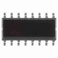
ST7FLITES5Y0M6TR STMicroelectronics, ST7FLITES5Y0M6TR Datasheet - Page 25

ST7FLITES5Y0M6TR
Manufacturer Part Number
ST7FLITES5Y0M6TR
Description
IC MCU 8BIT 1K FLASH 16-SOIC
Manufacturer
STMicroelectronics
Series
ST7r
Datasheet
1.ST7FLITES2Y0B6.pdf
(124 pages)
Specifications of ST7FLITES5Y0M6TR
Core Processor
ST7
Core Size
8-Bit
Speed
8MHz
Connectivity
SPI
Peripherals
LVD, POR, PWM, WDT
Number Of I /o
13
Program Memory Size
1KB (1K x 8)
Program Memory Type
FLASH
Ram Size
128 x 8
Voltage - Supply (vcc/vdd)
2.4 V ~ 5.5 V
Data Converters
A/D 5x10b
Oscillator Type
Internal
Operating Temperature
-40°C ~ 85°C
Package / Case
16-SOIC (3.9mm Width)
Processor Series
ST7FLITESx
Core
ST7
Data Bus Width
8 bit
Data Ram Size
128 B
Interface Type
SPI
Maximum Clock Frequency
8 MHz
Number Of Programmable I/os
13
Number Of Timers
2
Maximum Operating Temperature
+ 85 C
Mounting Style
SMD/SMT
Development Tools By Supplier
ST7FLIT0-IND/USB, ST7FLITE-SK/RAIS, ST7MDT10-DVP3, ST7MDT10-EMU3, STX-RLINK
Minimum Operating Temperature
- 40 C
On-chip Adc
8 bit, 5 Channel
For Use With
497-5858 - EVAL BOARD PLAYBACK ST7FLITE497-5049 - KIT STARTER RAISONANCE ST7FLITE
Lead Free Status / RoHS Status
Lead free / RoHS Compliant
Eeprom Size
-
Lead Free Status / Rohs Status
Details
Available stocks
Company
Part Number
Manufacturer
Quantity
Price
Figure 13. PLL Output Frequency Timing
Diagram
When the PLL is started, after reset or wakeup
from Halt mode or AWUFH mode, it outputs the
clock after a delay of t
When the PLL output signal reaches the operating
frequency, the LOCKED bit in the SICSCR register
is set. Full PLL accuracy (ACC
a stabilization time of t
13.3.4 Internal RC Oscillator and
Refer to
of the LOCKED bit in the SICSR register.
7.3 REGISTER DESCRIPTION
MAIN CLOCK CONTROL/STATUS REGISTER
(MCCSR)
Read / Write
Reset Value: 0000 0000 (00h)
Bits 7:2 = Reserved, must be kept cleared.
Table 5. Clock Register Map and Reset Values
4/8 x
input
freq.
Address
7
0
(Hex.)
0038h
0039h
t
STARTUP
section 8.4.4 on page 36
0
MCCSR
Reset Value
RCCR
Reset Value
Register
0
t
Label
LOCK
0
STARTUP
STAB
LOCKED bit set
0
CR7
7
0
1
(see
t
PLL
.
STAB
) is reached after
PLL)
0
for a description
Figure 13
CR6
MCO
6
0
1
SMS
t
and
0
CR5
5
0
1
Bit 1 = MCO Main Clock Out enable
This bit is read/write by software and cleared by
hardware after a reset. This bit allows to enable
the MCO output clock.
0: MCO clock disabled, I/O port free for general
1: MCO clock enabled.
Bit 0 = SMS Slow Mode select
This bit is read/write by software and cleared by
hardware after a reset. This bit selects the input
clock f
0: Normal mode (f
1: Slow mode (f
RC CONTROL REGISTER (RCCR)
Read / Write
Reset Value: 1111 1111 (FFh)
Bits 7:0 = CR[7:0] RC Oscillator Frequency Ad-
justment Bits
These bits must be written immediately after reset
to adjust the RC oscillator frequency and to obtain
an accuracy of 1%. The application can store the
correct value for each voltage range in EEPROM
and write it to this register at start-up.
00h = maximum available frequency
FFh = lowest available frequency
Note: To tune the oscillator, write a series of differ-
ent values in the register until the correct frequen-
cy is reached. The fastest method is to use a di-
chotomy starting with 80h.
CR7
purpose I/O.
7
CR4
4
0
1
OSC
CR6
or f
CR3
CR5
OSC
3
0
1
CPU =
ST7LITE0xY0, ST7LITESxY0
/32.
CPU =
CR4
f
OSC
CR2
f
OSC
2
0
1
/32)
CR3
CR2
MCO
CR1
1
0
1
CR1
SMS
CR0
25/124
0
0
1
CR0
0
1


