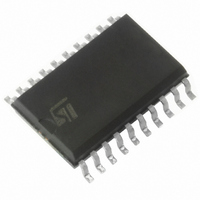
ST7FLIT10BF0M6 STMicroelectronics, ST7FLIT10BF0M6 Datasheet - Page 157

ST7FLIT10BF0M6
Manufacturer Part Number
ST7FLIT10BF0M6
Description
IC MCU 8BIT 2K FLASH 20-SOIC
Manufacturer
STMicroelectronics
Series
ST7r
Datasheet
1.ST7FLIT15BY1M6.pdf
(159 pages)
Specifications of ST7FLIT10BF0M6
Core Processor
ST7
Core Size
8-Bit
Speed
8MHz
Connectivity
SPI
Peripherals
LVD, POR, PWM, WDT
Number Of I /o
17
Program Memory Size
2KB (2K x 8)
Program Memory Type
FLASH
Ram Size
256 x 8
Voltage - Supply (vcc/vdd)
2.7 V ~ 5.5 V
Data Converters
A/D 7x10b
Oscillator Type
Internal
Operating Temperature
-40°C ~ 85°C
Package / Case
20-SOIC (7.5mm Width)
Processor Series
ST7FLIT1x
Core
ST7
Data Bus Width
8 bit
Data Ram Size
256 B
Interface Type
SPI
Maximum Clock Frequency
8 MHz
Number Of Programmable I/os
17
Number Of Timers
4
Operating Supply Voltage
2.7 V to 5.5 V
Maximum Operating Temperature
+ 85 C
Mounting Style
SMD/SMT
Development Tools By Supplier
ST7FLITE-SK/RAIS, ST7MDT10-DVP3, ST7MDT10-EMU3, STX-RLINK
Minimum Operating Temperature
- 40 C
On-chip Adc
10 bit, 7 Channel
For Use With
497-5049 - KIT STARTER RAISONANCE ST7FLITE
Lead Free Status / RoHS Status
Lead free / RoHS Compliant
Eeprom Size
-
Lead Free Status / Rohs Status
Details
Available stocks
Company
Part Number
Manufacturer
Quantity
Price
16 REVISION HISTORY
15-Sept-06
20-Dec-05
20-July-06
Date
Revision
1
2
3
Initial release on internet
Added reset default state in bold for RESET, PC0 and PC1 in
tion,” on page 7
Changed note below
DLING” on page 18
Modified note 3 in
ue and replaced h by b for LTCSR1, ATCSR and SICSR reset values
Added note to
Modified caution in
Added note 2 in “EXTERNAL INTERRUPT CONTROL REGISTER (EICR)” on page 38 and
changed “External Interrupt Function” on page 48
Removed references to true open drain in Table 8 on page 50, Table 9 on page 51 and notes
Replaced Auto reload timer 3 by Auto reload timer 4 in
Modified the BA bit description in the BREAKCR register in
Changed order of
graphs before
Modified
Modified bit names in the description of LTARR and LTCNTR registers in
page 81
Added important note in
tion in
Modified CINV bit description in
Changed LTCSR2 reset values in Table 2 on page 10 and in
Modified
Modified
Removed Vt
Modified
Modified
Modified
Modified temperature range in
Modified
Added note in
Removed figures “PLLx4 and PLLx8 Output vs CLKIN frequency”
Updated
Modified
Modified
Modified
Modified
Removed empty figure “Typical I
modified note 3
Modified temperature range in
Modified
Added “related Application notes” in
Removed EMC protection circuitry in
these components)
Modified ADC accuracy table in
Modified temperature range in
Modified Table 27 on page 150
Added note 3 to E
Modified
Modified
Updated
Removed QFN20 pinout and mechanical data.
Modified description of CNTR[11:0] bits in
Added “External Clock Source” on page 124 and
Modified Table 1.
section 11.6.4 on page 102
Section 11.3.3.2
section 13.2.2 on page 111
Section 13.3.1
section 13.3.4 on page 114
section 13.3.5 on page 114
section 13.3.5.1 on page 115
section 13.4.1 on page 121
section 13.5.4 on page 125
section 13.6 on page 126
Section 13.7.1
section 13.10.1 on page 137
Figure 108
section 13.9.1 on page 135
section 14.2 on page 148
section 15.2 on page 151
section 15.3 on page 153
POR
section 11.3.4 on page 81
section 13.5.3 on page 124
Figure 14 on page 26
min value in
Table 2, “Hardware Register Map,” on page
Section 11.3.3.2
D
section 7.2 on page 23
and E
(CPHA=1) and
Figure 9 on page 17
and
and
section 11.6.3 on page 100
L
in Table “ADC Accuracy with VDD=5.0V” on page 140
section 13.3.2 on page 112
section 13.7.2 on page 127
section 13.3.3.1 on page 113
section 13.3.5.3 on page 119
section 13.8.2 on page 130
Section
section 11.6.4 on page 102
PU
section 13.11 on page 139
and
vs. V
(part numbers in QFN20 package)
Figure 109 on page 138
section 13.11 on page 139
Figure 106 on page 136
(I
Main changes
(t
IO
13.12,
and
section 11.3.3.3 on page 80
su(SS),
DD
values)
and the last paragraph of “ACCESS ERROR HAN-
section 11.2.6 on page 72
with V
section 13.3.5.2 on page 117
Section 13.13
t
v(MO) and
IN
Figure 78 on page 124
=V
and added note to CHYST bit descrip-
SS”
section 11.2 on page 57
t
h(MO)
in
section 11.2.6 on page 70
section 13.8.1 on page 129
and
and
(device works correctly without
(t
section 11.3.6 on page 81
)
Table 1, “Device Pin Descrip-
10, changed LTICR reset val-
v(MO) ,
Figure 62 on page 101
section 13.14 on page 143
and removed two para-
t
h(MO)
section 11.3.6 on
)
ST7LITE1xB
157/159
and


