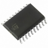
ST7FLIT10BF0M6 STMicroelectronics, ST7FLIT10BF0M6 Datasheet - Page 28

ST7FLIT10BF0M6
Manufacturer Part Number
ST7FLIT10BF0M6
Description
IC MCU 8BIT 2K FLASH 20-SOIC
Manufacturer
STMicroelectronics
Series
ST7r
Datasheet
1.ST7FLIT15BY1M6.pdf
(159 pages)
Specifications of ST7FLIT10BF0M6
Core Processor
ST7
Core Size
8-Bit
Speed
8MHz
Connectivity
SPI
Peripherals
LVD, POR, PWM, WDT
Number Of I /o
17
Program Memory Size
2KB (2K x 8)
Program Memory Type
FLASH
Ram Size
256 x 8
Voltage - Supply (vcc/vdd)
2.7 V ~ 5.5 V
Data Converters
A/D 7x10b
Oscillator Type
Internal
Operating Temperature
-40°C ~ 85°C
Package / Case
20-SOIC (7.5mm Width)
Processor Series
ST7FLIT1x
Core
ST7
Data Bus Width
8 bit
Data Ram Size
256 B
Interface Type
SPI
Maximum Clock Frequency
8 MHz
Number Of Programmable I/os
17
Number Of Timers
4
Operating Supply Voltage
2.7 V to 5.5 V
Maximum Operating Temperature
+ 85 C
Mounting Style
SMD/SMT
Development Tools By Supplier
ST7FLITE-SK/RAIS, ST7MDT10-DVP3, ST7MDT10-EMU3, STX-RLINK
Minimum Operating Temperature
- 40 C
On-chip Adc
10 bit, 7 Channel
For Use With
497-5049 - KIT STARTER RAISONANCE ST7FLITE
Lead Free Status / RoHS Status
Lead free / RoHS Compliant
Eeprom Size
-
Lead Free Status / Rohs Status
Details
Available stocks
Company
Part Number
Manufacturer
Quantity
Price
ST7LITE1xB
7.5 RESET SEQUENCE MANAGER (RSM)
7.5.1 Introduction
The reset sequence manager includes three RE-
SET sources as shown in
■
■
■
Note: A reset can also be triggered following the
detection of an illegal opcode or prebyte code. Re-
fer to
tails.
These sources act on the RESET pin and it is al-
ways kept low during the delay phase.
The RESET service routine vector is fixed at ad-
dresses FFFEh-FFFFh in the ST7 memory map.
The basic RESET sequence consists of 3 phases
as shown in
■
■
■
Caution: When the ST7 is unprogrammed or fully
erased, the Flash is blank and the RESET vector
is not programmed. For this reason, it is recom-
mended to keep the RESET pin in low state until
programming mode is entered, in order to avoid
unwanted behavior.
The 256 or 4096 CPU clock cycle delay allows the
oscillator to stabilise and ensures that recovery
has taken place from the Reset state. The shorter
or longer clock cycle delay is automatically select-
ed depending on the clock source chosen by op-
tion byte:
The RESET vector fetch phase duration is 2 clock
cycles.
28/159
1
External RESET source pulse
Internal LVD RESET (Low Voltage Detection)
Internal WATCHDOG RESET
Active Phase depending on the RESET source
256 or 4096 CPU clock cycle delay (see table
below)
RESET vector fetch
section 12.2.1 on page 107
Figure
15:
Figure
16:
for further de-
If the PLL is enabled by option byte, it outputs the
clock after an additional delay of t
Figure
Figure 15. RESET Sequence Phases
7.5.2 Asynchronous External RESET pin
The RESET pin is both an input and an open-drain
output with integrated R
This pull-up has no fixed value but varies in ac-
cordance with the input voltage. It can be pulled
low by external circuitry to reset the device. See
Electrical Characteristic section for more details.
A RESET signal originating from an external
source must have a duration of at least t
order to be recognized (see
tection is asynchronous and therefore the MCU
can enter reset state even in HALT mode.
Internal RC Oscillator
External clock (connected to CLKIN pin)
External Crystal/Ceramic Oscillator
(connected to OSC1/OSC2 pins)
Active Phase
13).
Clock Source
256 or 4096 CLOCK CYCLES
INTERNAL RESET
RESET
ON
weak pull-up resistor.
Figure
STARTUP
17). This de-
cycle delay
CPU clock
VECTOR
h(RSTL)in
FETCH
4096
256
256
(see
in


