Z8F0412SJ020SG Zilog, Z8F0412SJ020SG Datasheet - Page 192
Z8F0412SJ020SG
Manufacturer Part Number
Z8F0412SJ020SG
Description
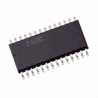
IC ENCORE MCU FLASH 4K 28SOIC
Manufacturer
Zilog
Series
Encore!® XP®r
Datasheet
1.Z8F08200100KIT.pdf
(264 pages)
Specifications of Z8F0412SJ020SG
Core Processor
Z8
Core Size
8-Bit
Speed
20MHz
Connectivity
I²C, IrDA, SPI, UART/USART
Peripherals
Brown-out Detect/Reset, POR, PWM, WDT
Number Of I /o
19
Program Memory Size
4KB (4K x 8)
Program Memory Type
FLASH
Ram Size
1K x 8
Voltage - Supply (vcc/vdd)
2.7 V ~ 3.6 V
Oscillator Type
Internal
Operating Temperature
0°C ~ 70°C
Package / Case
28-SOIC (7.5mm Width)
Processor Series
Z8F041xx
Core
eZ8
Data Bus Width
8 bit
Data Ram Size
1 KB
Interface Type
I2C, SPI, UART
Maximum Clock Frequency
20 MHz
Number Of Programmable I/os
19
Number Of Timers
2
Operating Supply Voltage
2.7 V to 3.6 V
Maximum Operating Temperature
+ 70 C
Mounting Style
SMD/SMT
Minimum Operating Temperature
0 C
Lead Free Status / RoHS Status
Lead free / RoHS Compliant
Eeprom Size
-
Data Converters
-
Lead Free Status / Rohs Status
Details
Other names
269-4107
Z8F0412SJ020SG
Z8F0412SJ020SG
Available stocks
Company
Part Number
Manufacturer
Quantity
Price

Part Number:
Z8F0412SJ020SG
Manufacturer:
ZILOG
Quantity:
20 000


PS022517-0508
•
•
•
•
•
Read OCD Control Register (05H)
reads the value of the OCDCTL register.
Write Program Counter (06H)
data that follows to the eZ8 CPU’s Program Counter. If the device is not in DEBUG
mode or if the Read Protect Option Bit is enabled, the Program Counter values are
discarded.
Read Program Counter (07H)
value in the eZ8 CPU’s Program Counter. If the device is not in DEBUG mode or if
the Read Protect Option Bit is enabled, this command returns
Write Register (08H)
Data can be written 1-256 bytes at a time (256 bytes can be written by setting size to
zero). If the device is not in DEBUG mode, the address and data values are discarded.
If the Read Protect Option Bit is enabled, then only writes to the Flash Control
Registers are allowed and all other register write data values are discarded.
Read Register (09H)
File. Data can be read 1-256 bytes at a time (256 bytes can be read by setting size to
zero). Reading peripheral control registers through the OCD does not effect peripheral
operation. For example, register bits that are normally cleared upon a read operation
will not be effected (WDTSTAT register is affected by OCD read register operation).
If the device is not in DEBUG mode or if the Read Protect Option Bit is enabled, this
command returns
DBG ← 04H
DBG ← OCDCTL[7:0]
DBG ← 05H
DBG → OCDCTL[7:0]
DBG ← 06H
DBG ← ProgramCounter[15:8]
DBG ← ProgramCounter[7:0]
DBG ← 07H
DBG → ProgramCounter[15:8]
DBG → ProgramCounter[7:0]
DBG ← 08H
DBG ← {4’h0,Register Address[11:8]}
DBG ← Register Address[7:0]
DBG ← Size[7:0]
DBG ← 1-256 data bytes
DBG ← 09H
DBG ← {4’h0,Register Address[11:8]
DBG ← Register Address[7:0]
DBG ← Size[7:0]
DBG → 1-256 data bytes
FFH
—The Write Register command writes data to the Register File.
—The Read Register command reads data from the Register
for all the data values.
—The Read Program Counter command reads the
—The Write Program Counter command writes the
—The Read OCD Control Register command
Z8 Encore! XP
Product Specification
FFFFH
®
.
On-Chip Debugger
F0822 Series
179
Related parts for Z8F0412SJ020SG
Image
Part Number
Description
Manufacturer
Datasheet
Request
R

Part Number:
Description:
Communication Controllers, ZILOG INTELLIGENT PERIPHERAL CONTROLLER (ZIP)
Manufacturer:
Zilog, Inc.
Datasheet:

Part Number:
Description:
KIT DEV FOR Z8 ENCORE 16K TO 64K
Manufacturer:
Zilog
Datasheet:

Part Number:
Description:
KIT DEV Z8 ENCORE XP 28-PIN
Manufacturer:
Zilog
Datasheet:

Part Number:
Description:
DEV KIT FOR Z8 ENCORE 8K/4K
Manufacturer:
Zilog
Datasheet:

Part Number:
Description:
KIT DEV Z8 ENCORE XP 28-PIN
Manufacturer:
Zilog
Datasheet:

Part Number:
Description:
DEV KIT FOR Z8 ENCORE 4K TO 8K
Manufacturer:
Zilog
Datasheet:
Part Number:
Description:
CMOS Z8 microcontroller. ROM 16 Kbytes, RAM 256 bytes, speed 16 MHz, 32 lines I/O, 3.0V to 5.5V
Manufacturer:
Zilog, Inc.
Datasheet:
Part Number:
Description:
Low-cost microcontroller. 512 bytes ROM, 61 bytes RAM, 8 MHz
Manufacturer:
Zilog, Inc.
Datasheet:
Part Number:
Description:
Z8 4K OTP Microcontroller
Manufacturer:
Zilog, Inc.
Datasheet:
Part Number:
Description:
CMOS SUPER8 ROMLESS MCU
Manufacturer:
Zilog, Inc.
Datasheet:
Part Number:
Description:
SL1866 CMOSZ8 OTP Microcontroller
Manufacturer:
Zilog, Inc.
Datasheet:
Part Number:
Description:
SL1866 CMOSZ8 OTP Microcontroller
Manufacturer:
Zilog, Inc.
Datasheet:
Part Number:
Description:
OTP (KB) = 1, RAM = 125, Speed = 12, I/O = 14, 8-bit Timers = 2, Comm Interfaces Other Features = Por, LV Protect, Voltage = 4.5-5.5V
Manufacturer:
Zilog, Inc.
Datasheet:
Part Number:
Description:
Manufacturer:
Zilog, Inc.
Datasheet: