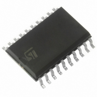
ST62T10CM6 STMicroelectronics, ST62T10CM6 Datasheet - Page 24

ST62T10CM6
Manufacturer Part Number
ST62T10CM6
Description
IC MCU 8BIT OTP 2K 20 SOIC
Manufacturer
STMicroelectronics
Series
ST6r
Datasheet
1.ST62T10CB6.pdf
(104 pages)
Specifications of ST62T10CM6
Core Processor
ST6
Core Size
8-Bit
Speed
8MHz
Peripherals
LVD, POR, WDT
Number Of I /o
12
Program Memory Size
2KB (2K x 8)
Program Memory Type
OTP
Ram Size
64 x 8
Voltage - Supply (vcc/vdd)
3 V ~ 6 V
Data Converters
A/D 8x8b
Oscillator Type
Internal
Operating Temperature
-40°C ~ 85°C
Package / Case
20-SOIC (7.5mm Width)
Cpu Family
ST6
Device Core Size
8b
Frequency (max)
8MHz
Total Internal Ram Size
64Byte
# I/os (max)
12
Number Of Timers - General Purpose
1
Operating Supply Voltage (typ)
3.3/5V
Operating Supply Voltage (max)
6V
Operating Supply Voltage (min)
3V
On-chip Adc
8-chx8-bit
Instruction Set Architecture
CISC
Operating Temp Range
-40C to 85C
Operating Temperature Classification
Industrial
Mounting
Surface Mount
Pin Count
20
Package Type
SOP
Processor Series
ST62T1x
Core
ST6
Data Bus Width
8 bit
Data Ram Size
64 B
Maximum Clock Frequency
8 MHz
Number Of Programmable I/os
12
Number Of Timers
1
Operating Supply Voltage
3 V to 6 V
Maximum Operating Temperature
+ 85 C
Mounting Style
SMD/SMT
Development Tools By Supplier
ST622XC-KIT/110, ST62GP-EMU2, ST62E2XC-EPB/110, ST62E6XC-EPB/US, STREALIZER-II
Minimum Operating Temperature
- 40 C
Controller Family/series
ST6
No. Of I/o's
12
Ram Memory Size
64Byte
Cpu Speed
8MHz
No. Of Timers
1
Rohs Compliant
Yes
Lead Free Status / RoHS Status
Lead free / RoHS Compliant
Eeprom Size
-
Connectivity
-
Lead Free Status / Rohs Status
Compliant
Other names
497-2097-5
Available stocks
Company
Part Number
Manufacturer
Quantity
Price
Part Number:
ST62T10CM6
Manufacturer:
ST
Quantity:
20 000
ST6208C/ST6209C/ST6210C/ST6220C
5.3 RESET
5.3.1 Introduction
The MCU can be reset in three ways:
■
■
■
5.3.2 RESET Sequence
The basic RESET sequence consists of 3 main
phases:
■
■
■
The reset delay allows the oscillator to stabilise
and ensures that recovery has taken place from
the Reset state.
Figure 13. RESET Sequence
24/104
1
A low pulse input on the RESET pin
Internal Watchdog reset
Internal Low Voltage Detector (LVD) reset
Internal (watchdog or LVD) or external Reset
event
A delay of 2048 clock (f
RESET vector fetch
WATCHDOG
RESET PIN
INTERNAL
RESET
RESET
RESET
LVD
V
V
IT+
IT-
V
RUN
DD
INT
RESET
) cycles
RUN
RESET
WATCHDOG UNDERFLOW
The RESET vector fetch phase duration is 2 clock
cycles.
When a reset occurs:
– The stack is cleared
– The PC is loaded with the address of the Reset
A jump to the beginning of the user program must
be coded at this address.
– The interrupt flag is automatically set, so that the
vector. It is located in program ROM starting at
address 0FFEh.
CPU is in Non Maskable Interrupt mode. This
prevents the initialization routine from being in-
terrupted. The initialization routine should there-
fore be terminated by a RETI instruction, in order
to go back to normal mode.
RUN
RESET
2048 CLOCK CYCLE (f INT ) DELAY
RUN


