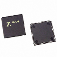
Z8F1622VS020SG Zilog, Z8F1622VS020SG Datasheet - Page 142

Z8F1622VS020SG
Manufacturer Part Number
Z8F1622VS020SG
Description
IC ENCORE MCU FLASH 16K 68PLCC
Manufacturer
Zilog
Series
Encore!® XP®r
Specifications of Z8F1622VS020SG
Core Processor
Z8
Core Size
8-Bit
Speed
20MHz
Connectivity
I²C, IrDA, SPI, UART/USART
Peripherals
Brown-out Detect/Reset, DMA, POR, PWM, WDT
Number Of I /o
46
Program Memory Size
16KB (16K x 8)
Program Memory Type
FLASH
Ram Size
2K x 8
Voltage - Supply (vcc/vdd)
3 V ~ 3.6 V
Data Converters
A/D 12x10b
Oscillator Type
Internal
Operating Temperature
0°C ~ 70°C
Package / Case
68-LCC (J-Lead)
Processor Series
Z8F162x
Core
eZ8
Data Bus Width
8 bit
Data Ram Size
2 KB
Interface Type
I2C, SPI, UART
Maximum Clock Frequency
20 MHz
Number Of Programmable I/os
46
Number Of Timers
4
Operating Supply Voltage
3 V to 3.6 V
Maximum Operating Temperature
+ 70 C
Mounting Style
SMD/SMT
Minimum Operating Temperature
0 C
On-chip Adc
10 bit, 12 Channel
Lead Free Status / RoHS Status
Lead free / RoHS Compliant
Eeprom Size
-
Lead Free Status / Rohs Status
Details
Other names
269-4243
Z8F1622VS020SG
Z8F1622VS020SG
Available stocks
Company
Part Number
Manufacturer
Quantity
Price
- Current page: 142 of 297
- Download datasheet (9Mb)
PS019921-0308
SPI Clock Phase and Polarity Control
The Master and Slave are each capable of exchanging a character of data during a
sequence of NUMBITS clock cycles (see NUMBITS field in the
page 136). In both Master and Slave SPI devices, data is shifted on one edge of the SCK
and is sampled on the opposite edge where data is stable. Edge polarity is determined by
the SPI phase and polarity control.
Slave Select
The active Low Slave Select (SS) input signal selects a Slave SPI device. SS must be Low
prior to all data communication to and from the Slave device. SS must stay Low for the
full duration of each character transferred. The SS signal may stay Low during the transfer
of multiple characters or may deassert between each character.
When the SPI is configured as the only Master in an SPI system, the SS pin can be set as
either an input or an output. Other GPIO output pins can also be employed to select exter-
nal SPI Slave devices.
When the SPI is configured as one Master in a multi-master SPI system, the SS pin must
be set as an input. The SS input signal on the Master must be High. If the SS signal goes
Low (indicating another Master is driving the SPI bus), a Collision error Flag is set in the
SPI Status register.
The SPI supports four combinations of serial clock phase and polarity using two bits in the
SPI Control register. The clock polarity bit, CLKPOL, selects an active high or active Low
clock and has no effect on the transfer format.
Polarity Operation parameters. The clock phase bit, PHASE, selects one of two fundamen-
tally different transfer formats. For proper data transmission, the clock phase and polarity
must be identical for the SPI Master and the SPI Slave. The Master always places data on
the MOSI line a half-cycle before the receive clock edge (SCK signal), in order for the
Slave to latch the data.
Table 62. SPI Clock Phase (PHASE) and Clock Polarity (CLKPOL) Operation
PHASE
0
0
1
1
CLKPOL
0
1
0
1
SCK Transmit
Falling
Falling
Rising
Rising
Edge
Table 62
SCK Receive
Z8 Encore! XP
lists the SPI Clock Phase and
Falling
Falling
Rising
Rising
Edge
Product Specification
SPI Mode Register
Serial Peripheral Interface
®
F64XX Series
SCK Idle
State
High
High
Low
Low
on
128
Related parts for Z8F1622VS020SG
Image
Part Number
Description
Manufacturer
Datasheet
Request
R

Part Number:
Description:
Communication Controllers, ZILOG INTELLIGENT PERIPHERAL CONTROLLER (ZIP)
Manufacturer:
Zilog, Inc.
Datasheet:

Part Number:
Description:
KIT DEV FOR Z8 ENCORE 16K TO 64K
Manufacturer:
Zilog
Datasheet:

Part Number:
Description:
KIT DEV Z8 ENCORE XP 28-PIN
Manufacturer:
Zilog
Datasheet:

Part Number:
Description:
DEV KIT FOR Z8 ENCORE 8K/4K
Manufacturer:
Zilog
Datasheet:

Part Number:
Description:
KIT DEV Z8 ENCORE XP 28-PIN
Manufacturer:
Zilog
Datasheet:

Part Number:
Description:
DEV KIT FOR Z8 ENCORE 4K TO 8K
Manufacturer:
Zilog
Datasheet:

Part Number:
Description:
CMOS Z8 microcontroller. ROM 16 Kbytes, RAM 256 bytes, speed 16 MHz, 32 lines I/O, 3.0V to 5.5V
Manufacturer:
Zilog, Inc.
Datasheet:

Part Number:
Description:
Low-cost microcontroller. 512 bytes ROM, 61 bytes RAM, 8 MHz
Manufacturer:
Zilog, Inc.
Datasheet:

Part Number:
Description:
Z8 4K OTP Microcontroller
Manufacturer:
Zilog, Inc.
Datasheet:

Part Number:
Description:
CMOS SUPER8 ROMLESS MCU
Manufacturer:
Zilog, Inc.
Datasheet:

Part Number:
Description:
SL1866 CMOSZ8 OTP Microcontroller
Manufacturer:
Zilog, Inc.
Datasheet:

Part Number:
Description:
SL1866 CMOSZ8 OTP Microcontroller
Manufacturer:
Zilog, Inc.
Datasheet:

Part Number:
Description:
OTP (KB) = 1, RAM = 125, Speed = 12, I/O = 14, 8-bit Timers = 2, Comm Interfaces Other Features = Por, LV Protect, Voltage = 4.5-5.5V
Manufacturer:
Zilog, Inc.
Datasheet:

Part Number:
Description:
Manufacturer:
Zilog, Inc.
Datasheet:


