ST7FMC1K2T6/TR STMicroelectronics, ST7FMC1K2T6/TR Datasheet - Page 239
ST7FMC1K2T6/TR
Manufacturer Part Number
ST7FMC1K2T6/TR
Description
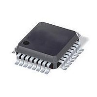
IC MCU 8BIT 8K FLASH 32-LQFP
Manufacturer
STMicroelectronics
Series
ST7r
Datasheet
1.ST7FMC2S4T6.pdf
(309 pages)
Specifications of ST7FMC1K2T6/TR
Core Processor
ST7
Core Size
8-Bit
Speed
8MHz
Connectivity
LINSCI
Peripherals
LVD, Motor Control PWM, POR, PWM, WDT
Number Of I /o
17
Program Memory Size
8KB (8K x 8)
Program Memory Type
FLASH
Ram Size
384 x 8
Voltage - Supply (vcc/vdd)
3.8 V ~ 5.5 V
Data Converters
A/D 16x10b
Oscillator Type
Internal
Operating Temperature
-40°C ~ 85°C
Package / Case
32-LQFP
Processor Series
ST7FMC1x
Core
ST7
Data Bus Width
8 bit
Data Ram Size
384 B
Interface Type
SCI, SPI
Maximum Clock Frequency
8 MHz
Number Of Programmable I/os
17
Number Of Timers
3
Maximum Operating Temperature
+ 85 C
Mounting Style
SMD/SMT
Development Tools By Supplier
ST7MC-KIT/BLDC, ST7MDT50-EMU3, STX-RLINK
Minimum Operating Temperature
- 40 C
On-chip Adc
10 bit, 16 Channel
For Use With
497-8402 - BOARD EVAL COMPLETE INVERTER497-8400 - KIT IGBT PWR MODULE CTRL ST7MC497-4734 - EVAL KIT 3KW POWER DRIVER BOARD497-4733 - EVAL KIT 1KW POWER DRIVER BOARD497-4732 - EVAL KIT 300W POWER DRIVER BOARD497-4731 - EVAL KIT PWR DRIVER CONTROL BRD
Lead Free Status / RoHS Status
Lead free / RoHS Compliant
Eeprom Size
-
Lead Free Status / Rohs Status
Details
Available stocks
Company
Part Number
Manufacturer
Quantity
Price
Company:

Part Number:
ST7FMC1K2T6/TR
Manufacturer:
STMicroelectronics
Quantity:
10 000


10-BIT A/D CONVERTER (ADC) (Cont’d)
10.8.6 Register Description
CONTROL/STATUS REGISTER (ADCCSR)
Read/Write (Except bit 7 read only)
Reset Value: 0000 0000 (00h)
Bit 7 = EOC End of Conversion
This bit is set by hardware. It is cleared by soft-
ware reading the ADCDRMSB register.
0: Conversion is not complete
1: Conversion complete
Bit 6:5 = PRSC[1:0] ADC clock prescaler selection
These bits are set and cleared by software.
Bit 4 = ADON A/D Converter on
This bit is set and cleared by software.
0: Disable ADC and stop conversion
1: Enable ADC and start conversion
Bit 3:0 = CS[3:0] Channel Selection
These bits are set and cleared by software. They
select the analog input to convert.
*The number of channels is device dependent. Refer to
the device pinout description.
EOC PRSC1 PRSC0 ADON
7
Channel Pin*
4MHz
2MHz
1MHz
f
ADC
AIN10
AIN11
AIN12
AIN13
AIN14
AIN15
AIN0
AIN1
AIN2
AIN3
AIN4
AIN5
AIN6
AIN7
AIN8
AIN9
PRSC1
CH3
0
0
1
0
0
0
0
0
0
0
0
1
1
1
1
1
1
1
1
CS3
CH2
0
0
0
0
1
1
1
1
0
0
0
0
1
1
1
1
CS2
CH1
PRSC0
CS1
0
0
1
1
0
0
1
1
0
0
1
1
0
0
1
1
0
1
0
CH0
CS0
0
1
0
1
0
1
0
1
0
1
0
1
0
1
0
1
0
DATA REGISTER (ADCDRMSB)
Read Only
Reset Value: 0000 0000 (00h)
Bit 7:0 = D[9:2] MSB of Analog Converted Value
This register contains the MSB of the converted
analog value.
DATA REGISTER (ADCDRLSB)
Read Only
Reset Value: 0000 0000 (00h)
Bit 7:2 = Reserved. Forced by hardware to 0.
Bit 1:0 = D[1:0] LSB of Analog Converted Value
This register contains the LSB of the converted an-
alog value.
D9
7
7
0
D8
0
D7
0
D6
0
ST7MC1xx/ST7MC2xx
D5
0
D4
0
D3
D1
239/309
D2
D0
0
0
Related parts for ST7FMC1K2T6/TR
Image
Part Number
Description
Manufacturer
Datasheet
Request
R

Part Number:
Description:
STMicroelectronics [RIPPLE-CARRY BINARY COUNTER/DIVIDERS]
Manufacturer:
STMicroelectronics
Datasheet:
Part Number:
Description:
STMicroelectronics [LIQUID-CRYSTAL DISPLAY DRIVERS]
Manufacturer:
STMicroelectronics
Datasheet:

Part Number:
Description:
BOARD EVAL FOR MEMS SENSORS
Manufacturer:
STMicroelectronics
Datasheet:
Part Number:
Description:
NPN TRANSISTOR POWER MODULE
Manufacturer:
STMicroelectronics
Datasheet:
Part Number:
Description:
TURBOSWITCH ULTRA-FAST HIGH VOLTAGE DIODE
Manufacturer:
STMicroelectronics
Datasheet:
Part Number:
Description:
Manufacturer:
STMicroelectronics
Datasheet:
Part Number:
Description:
DIODE / SCR MODULE
Manufacturer:
STMicroelectronics
Datasheet:
Part Number:
Description:
DIODE / SCR MODULE
Manufacturer:
STMicroelectronics
Datasheet:
Part Number:
Description:
Search -----> STE16N100
Manufacturer:
STMicroelectronics
Datasheet:
Part Number:
Description:
Search ---> STE53NA50
Manufacturer:
STMicroelectronics
Datasheet:
Part Number:
Description:
NPN Transistor Power Module
Manufacturer:
STMicroelectronics
Datasheet:
Part Number:
Description:
DIODE / SCR MODULE
Manufacturer:
STMicroelectronics
Datasheet: