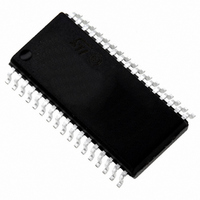
ST72F63BK4M1 STMicroelectronics, ST72F63BK4M1 Datasheet - Page 70

ST72F63BK4M1
Manufacturer Part Number
ST72F63BK4M1
Description
IC MCU 8BIT LS 16K 34-SOIC
Manufacturer
STMicroelectronics
Series
ST7r
Datasheet
1.ST72F63BD6U1TR.pdf
(186 pages)
Specifications of ST72F63BK4M1
Core Processor
ST7
Core Size
8-Bit
Speed
8MHz
Connectivity
I²C, SCI, USB
Peripherals
DMA, LVD, POR, PWM, WDT
Number Of I /o
19
Program Memory Size
16KB (16K x 8)
Program Memory Type
FLASH
Ram Size
512 x 8
Voltage - Supply (vcc/vdd)
4 V ~ 5.5 V
Data Converters
A/D 8x8b
Oscillator Type
Internal
Operating Temperature
0°C ~ 70°C
Package / Case
34-SOIC (7.5mm Width)
Processor Series
ST72F6x
Core
ST7
Data Bus Width
8 bit
Data Ram Size
512 B
Interface Type
I2C, SCI, USB
Maximum Clock Frequency
8 MHz
Number Of Programmable I/os
27
Number Of Timers
2 x 16 bit
Operating Supply Voltage
4 V to 5.5 V
Maximum Operating Temperature
+ 70 C
Mounting Style
SMD/SMT
Development Tools By Supplier
ST7MDTU3-EPB/US, ST72F63B-SK/RAIS, ST7MDTU3-EMU3, STX-RLINK
Minimum Operating Temperature
0 C
On-chip Adc
8 bit
For Use With
497-5521 - EVAL BOARD LOW SPEED USB
Lead Free Status / RoHS Status
Lead free / RoHS Compliant
Eeprom Size
-
Lead Free Status / Rohs Status
Details
Other names
497-2115-5
Available stocks
Company
Part Number
Manufacturer
Quantity
Price
Part Number:
ST72F63BK4M1
Manufacturer:
ST
Quantity:
20 000
On-chip peripherals
70/186
Figure 39. Pulse Width modulation mode timing with 2 output Compare functions
1. OC1R = 2ED0h, OC2R = 34E2, OLVL1 = 0, OLVL2 = 1
On timers with only one output Compare register, a fixed frequency PWM signal can be
generated using the output compare and the counter overflow to define the pulse length.
Pulse width modulation mode
Pulse width modulation (PWM) mode enables the generation of a signal with a frequency
and pulse length determined by the value of the OC1R and OC2R registers.
Pulse Width Modulation mode uses the complete output Compare 1 function plus the OC2R
register, and so this functionality can not be used when PWM mode is activated.
In PWM mode, double buffering is implemented on the output compare registers. Any new
values written in the OC1R and OC2R registers are taken into account only at the end of the
PWM period (OC2) to avoid spikes on the PWM output pin (OCMP1).
Procedure
To use Pulse Width Modulation mode:
1.
2.
3.
4.
Load the OC2R register with the value corresponding to the period of the signal using
the formula in the opposite column.
Load the OC1R register with the value corresponding to the period of the pulse if
(OLVL1 = 0 and OLVL2 = 1) using the formula in the opposite column.
Select the following in the CR1 register:
–
–
Select the following in the CR2 register:
–
–
–
Using the OLVL1 bit, select the level to be applied to the OCMP1 pin after a
successful comparison with the OC1R register.
Using the OLVL2 bit, select the level to be applied to the OCMP1 pin after a
successful comparison with the OC2R register.
Set OC1E bit: the OCMP1 pin is then dedicated to the output compare 1 function.
Set the PWM bit.
Select the timer clock (CC[1:0]) (see
COUNTER 34E2
OCMP1
compare2
FFFC FFFD FFFE
Doc ID 7516 Rev 8
OLVL2
Table
compare1
2ED0 2ED1 2ED2
24).
OLVL1
compare2
34E2
OLVL2
FFFC
ST7263Bxx


