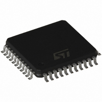
ST72F361J7T3 STMicroelectronics, ST72F361J7T3 Datasheet - Page 151

ST72F361J7T3
Manufacturer Part Number
ST72F361J7T3
Description
IC MCU 8BIT 48K FLASH 44-LQFP
Manufacturer
STMicroelectronics
Series
ST7r
Datasheet
1.ST72F361K6T6.pdf
(225 pages)
Specifications of ST72F361J7T3
Core Processor
ST7
Core Size
8-Bit
Speed
8MHz
Connectivity
LINSCI, SPI
Peripherals
LVD, POR, PWM, WDT
Number Of I /o
32
Program Memory Size
48KB (48K x 8)
Program Memory Type
FLASH
Ram Size
2K x 8
Voltage - Supply (vcc/vdd)
3.8 V ~ 5.5 V
Data Converters
A/D 16x10b
Oscillator Type
External
Operating Temperature
-40°C ~ 125°C
Package / Case
44-LQFP
Processor Series
ST72F3x
Core
ST7
Data Bus Width
8 bit
Data Ram Size
2 KB
Interface Type
LINSCI, SPI
Maximum Clock Frequency
8 MHz
Number Of Programmable I/os
34
Number Of Timers
2
Maximum Operating Temperature
+ 125 C
Mounting Style
SMD/SMT
Development Tools By Supplier
ST72F36X-SK/RAIS, STX-RLINK
Minimum Operating Temperature
- 40 C
On-chip Adc
10 bit, 11 Channel
Lead Free Status / RoHS Status
Lead free / RoHS Compliant
Eeprom Size
-
Lead Free Status / Rohs Status
Details
Available stocks
Company
Part Number
Manufacturer
Quantity
Price
Company:
Part Number:
ST72F361J7T3
Manufacturer:
STMicroelectronics
Quantity:
10 000
- Current page: 151 of 225
- Download datasheet (8Mb)
10.8 LINSCI SERIAL COMMUNICATION INTERFACE (LIN Master Only)
10.8.1 Introduction
The Serial Communications Interface (SCI) offers
a flexible means of full-duplex data exchange with
external equipment requiring an industry standard
NRZ asynchronous serial data format. The SCI of-
fers a very wide range of baud rates using two
baud rate generator systems.
10.8.2 Main Features
■
■
■
■
■
■
■
■
■
■
■
■
■
■
■
– Address bit (MSB)
– Idle line
– Overrun error
– Noise error
– Frame error
– Parity error
– Transmit data register empty
– Transmission complete
– Receive data register full
– Idle line received
– Overrun error detected
– Transmits parity bit
– Checks parity of received data byte
Full duplex, asynchronous communications
NRZ standard format (Mark/Space)
Dual baud rate generator systems
Independently programmable transmit and
receive baud rates up to 500K baud.
Programmable data word length (8 or 9 bits)
Receive buffer full, Transmit buffer empty and
End of Transmission flags
2 receiver wake-up modes:
Muting function for multiprocessor configurations
Separate enable bits for Transmitter and
Receiver
4 error detection flags:
5 interrupt sources with flags:
Transmitter clock output
Parity control:
Reduced power consumption mode
LIN Synch Break send capability
10.8.3 General Description
The interface is externally connected to another
device by three pins (see
Any SCI bidirectional communication requires a
minimum of two pins: Receive Data In (RDI) and
Transmit Data Out (TDO):
– SCLK: Transmitter clock output. This pin outputs
– TDO: Transmit Data Output. When the transmit-
– RDI: Receive Data Input is the serial data input.
Through these pins, serial data is transmitted and
received as frames comprising:
– An Idle Line prior to transmission or reception
– A start bit
– A data word (8 or 9 bits) least significant bit first
– A Stop bit indicating that the frame is complete.
This interface uses two types of baud rate generator:
– A conventional type for commonly-used baud
– An extended type with a prescaler offering a very
the transmitter data clock for synchronous trans-
mission (no clock pulses on start bit and stop bit,
and a software option to send a clock pulse on
the last data bit). This can be used to control pe-
ripherals that have shift registers (e.g. LCD driv-
ers). The clock phase and polarity are software
programmable.
ter is disabled, the output pin returns to its I/O
port configuration. When the transmitter is ena-
bled and nothing is to be transmitted, the TDO
pin is at high level.
Oversampling techniques are used for data re-
covery by discriminating between valid incoming
data and noise.
rates,
wide range of baud rates even with non-standard
oscillator frequencies.
Figure 88 on page
ST72361
151/225
153).
Related parts for ST72F361J7T3
Image
Part Number
Description
Manufacturer
Datasheet
Request
R

Part Number:
Description:
STMicroelectronics [RIPPLE-CARRY BINARY COUNTER/DIVIDERS]
Manufacturer:
STMicroelectronics
Datasheet:

Part Number:
Description:
STMicroelectronics [LIQUID-CRYSTAL DISPLAY DRIVERS]
Manufacturer:
STMicroelectronics
Datasheet:

Part Number:
Description:
BOARD EVAL FOR MEMS SENSORS
Manufacturer:
STMicroelectronics
Datasheet:

Part Number:
Description:
NPN TRANSISTOR POWER MODULE
Manufacturer:
STMicroelectronics
Datasheet:

Part Number:
Description:
TURBOSWITCH ULTRA-FAST HIGH VOLTAGE DIODE
Manufacturer:
STMicroelectronics
Datasheet:

Part Number:
Description:
Manufacturer:
STMicroelectronics
Datasheet:

Part Number:
Description:
DIODE / SCR MODULE
Manufacturer:
STMicroelectronics
Datasheet:

Part Number:
Description:
DIODE / SCR MODULE
Manufacturer:
STMicroelectronics
Datasheet:

Part Number:
Description:
Search -----> STE16N100
Manufacturer:
STMicroelectronics
Datasheet:

Part Number:
Description:
Search ---> STE53NA50
Manufacturer:
STMicroelectronics
Datasheet:

Part Number:
Description:
NPN Transistor Power Module
Manufacturer:
STMicroelectronics
Datasheet:

Part Number:
Description:
DIODE / SCR MODULE
Manufacturer:
STMicroelectronics
Datasheet:


