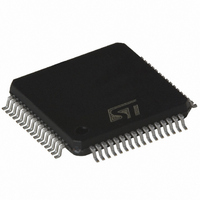
ST72F321AR6T6 STMicroelectronics, ST72F321AR6T6 Datasheet - Page 186

ST72F321AR6T6
Manufacturer Part Number
ST72F321AR6T6
Description
MCU 8BIT 32KB FLASH 64TQFP
Manufacturer
STMicroelectronics
Series
ST7r
Datasheet
1.ST72F321AR7T6.pdf
(193 pages)
Specifications of ST72F321AR6T6
Core Processor
ST7
Core Size
8-Bit
Speed
8MHz
Connectivity
I²C, SCI, SPI
Peripherals
LVD, POR, PWM, WDT
Number Of I /o
48
Program Memory Size
32KB (32K x 8)
Program Memory Type
FLASH
Ram Size
1K x 8
Voltage - Supply (vcc/vdd)
3.8 V ~ 5.5 V
Data Converters
A/D 16x10b
Oscillator Type
Internal
Operating Temperature
-40°C ~ 85°C
Package / Case
64-TQFP, 64-VQFP
Processor Series
ST72F3x
Core
ST7
Data Bus Width
8 bit
Data Ram Size
1024 B
Interface Type
I2C, SCI, SPI
Maximum Clock Frequency
8 MHz
Number Of Programmable I/os
48
Number Of Timers
5
Operating Supply Voltage
3.8 V to 5.5 V
Maximum Operating Temperature
+ 85 C
Mounting Style
SMD/SMT
Development Tools By Supplier
ST7F521-IND/USB, ST7232X-EVAL, ST7MDT20-DVP3, ST7MDT20J-EMU3, ST7MDT20M-EMU3, STX-RLINK
Minimum Operating Temperature
- 40 C
On-chip Adc
10 bit
Lead Free Status / RoHS Status
Lead free / RoHS Compliant
Eeprom Size
-
Lead Free Status / Rohs Status
Details
Other names
497-4842
Available stocks
Company
Part Number
Manufacturer
Quantity
Price
Company:
Part Number:
ST72F321AR6T6
Manufacturer:
STMicroelectronics
Quantity:
10 000
Part Number:
ST72F321AR6T6
Manufacturer:
ST
Quantity:
20 000
ST72321Rx ST72321ARx ST72321Jx
15 KNOWN LIMITATIONS
15.1 ALL FLASH AND ROM DEVICES
15.1.1 External RC option
The External RC clock source option described in
previous datasheet revisions is no longer support-
ed and has been removed from this specification.
15.1.2 Safe Connection of OSC1/OSC2 Pins
The OSC1 and/or OSC2 pins must not be left un-
connected otherwise the ST7 main oscillator may
start and, in this configuration, could generate an
f
maximum (>16MHz.), putting the ST7 in an un-
safe/undefined state. Refer to
25.
15.1.3 Reset pin protection with LVD Enabled
As mentioned in note 2 below
160, when the LVD is enabled, it is recommended
not to connect a pull-up resistor or capacitor. A
10nF pull-down capacitor is required to filter noise
on the reset line.
15.1.4 Unexpected Reset Fetch
If an interrupt request occurs while a “POP CC” in-
struction is executed, the interrupt controller does
not recognise the source of the interrupt and, by
default, passes the RESET vector address to the
CPU.
Workaround
To solve this issue, a “POP CC” instruction must
always be preceded by a “SIM” instruction.
15.1.5 External interrupt missed
To avoid any risk if generating a parasitic interrupt,
the edge detector is automatically disabled for one
clock cycle during an access to either DDR and
OR. Any input signal edge during this period will
not be detected and will not generate an interrupt.
This case can typically occur if the application re-
freshes the port configuration registers at intervals
during runtime.
Workaround
The workaround is based on software checking
the level on the interrupt pin before and after writ-
ing to the PxOR or PxDDR registers. If there is a
level change (depending on the sensitivity pro-
grammed for this pin) the interrupt routine is in-
voked using the call instruction with three extra
PUSH instructions before executing the interrupt
routine (this is to make the call compatible with the
IRET instruction at the end of the interrupt service
routine).
186/193
OSC
clock frequency in excess of the allowed
section 6.2 on page
Figure 89 on page
But detection of the level change does not make
sure that edge occurs during the critical 1 cycle du-
ration and the interrupt has been missed. This may
lead to occurrence of same interrupt twice (one
hardware and another with software call).
To avoid this, a semaphore is set to '1' before
checking the level change. The semaphore is
changed to level '0' inside the interrupt routine.
When a level change is detected, the semaphore
status is checked and if it is '1' this means that the
last interrupt has been missed. In this case, the in-
terrupt routine is invoked with the call instruction.
There is another possible case i.e. if writing to
PxOR or PxDDR is done with global interrupts dis-
abled (interrupt mask bit set). In this case, the
semaphore is changed to '1' when the level
change is detected. Detecting a missed interrupt is
done after the global interrupts are enabled (inter-
rupt mask bit reset) and by checking the status of
the semaphore. If it is '1' this means that the last
interrupt was missed and the interrupt routine is in-
voked with the call instruction.
To implement the workaround, the following soft-
ware sequence is to be followed for writing into the
PxOR/PxDDR registers. The example is for for
Port PF1 with falling edge interrupt sensitivity. The
software sequence is given for both cases (global
interrupt disabled/enabled).
Case 1: Writing to PxOR or PxDDR with Global In-
terrupts Enabled:
LD A,#01
LD sema,A
LD A,PFDR
AND A,#02
LD X,A
PxOR/PxDDR
LD A,#$90
LD PFDDR,A ; Write to PFDDR
LD A,#$ff
LD PFOR,A
LD A,PFDR
AND A,#02
LD Y,A
PxOR/PxDDR
LD A,X
cp A,#02
jrne OUT
; set the semaphore to '1'
; store the level before writing to
; store the level after writing to
; check for falling edge
; Write to PFOR


