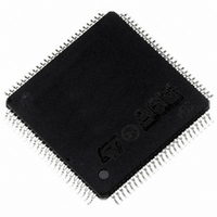
ST10R272LT1 STMicroelectronics, ST10R272LT1 Datasheet - Page 49

ST10R272LT1
Manufacturer Part Number
ST10R272LT1
Description
MCU 16BIT ROMLESS LV 100-TQFP
Manufacturer
STMicroelectronics
Series
ST10r
Datasheet
1.ST10R272LT1TR.pdf
(77 pages)
Specifications of ST10R272LT1
Core Processor
ST10
Core Size
16-Bit
Speed
50MHz
Connectivity
EBI/EMI, SSP, UART/USART
Peripherals
POR, PWM, WDT
Number Of I /o
77
Program Memory Type
ROMless
Ram Size
1K x 8
Voltage - Supply (vcc/vdd)
3 V ~ 3.6 V
Oscillator Type
Internal
Operating Temperature
0°C ~ 70°C
Package / Case
100-TQFP, 100-VQFP
Controller Family/series
ST10
No. Of I/o's
77
Ram Memory Size
1KB
Cpu Speed
50MHz
No. Of Timers
5
Embedded Interface Type
SPI, USART
No. Of Pwm Channels
1
Rohs Compliant
Yes
Processor Series
ST10R2x
Core
ST10
Data Bus Width
16 bit
Data Ram Size
1 KB
Interface Type
SSP, USART
Maximum Clock Frequency
50 MHz
Number Of Programmable I/os
77
Number Of Timers
5
Maximum Operating Temperature
+ 70 C
Mounting Style
SMD/SMT
Minimum Operating Temperature
0 C
On-chip Adc
16 bit
Case
QFP
Lead Free Status / RoHS Status
Lead free / RoHS Compliant
Eeprom Size
-
Program Memory Size
-
Data Converters
-
Lead Free Status / Rohs Status
Details
Available stocks
Company
Part Number
Manufacturer
Quantity
Price
Company:
Part Number:
ST10R272LT1
Manufacturer:
PANASONIC
Quantity:
30 000
Part Number:
ST10R272LT1
Manufacturer:
ST
Quantity:
20 000
Company:
Part Number:
ST10R272LT1/TR
Manufacturer:
STMicroelectronics
Quantity:
10 000
Note
Note that if the bit OWDDIS in SYSCON register is cleared, the PLL runs on its free-running
frequency and delivers the clock signal for the Oscillator Watchdog. If bit OWDDIS is set, then
the PLL is switched off.
Oscillator Watchdog (OWD)
When the clock option selected is direct drive or direct drive with prescaler, in order to provide
a fail safe mechanism in case of a loss of the external clock, an oscillator watchdog is
implemented as an additional functionality of the PLL circuitry. This oscillator watchdog
operates as follows:
After a reset, the Oscillator Watchdog is enabled by default. To disable the OWD, set bit 4 of
SYSCON register OWDDIS.
When the OWD is enabled, the PLL runs on its free-running frequency and increments the
Oscillator Watchdog counter. On each transition of the XTAL1 pin, the Oscillator Watchdog is
cleared. If an external clock failure occurs, then the Oscillator Watchdog counter overflows
(after 16 PLL clock cycles). The CPU clock signal will be switched to the PLL free-running
clock signal, and the Oscillator Watchdog Interrupt Request (XP3INT) is flagged. The CPU
clock will not switch back to the external clock even if a valid external clock exits on XTAL1 pin.
Only a hardware reset can switch the CPU clock source back to direct clock input.
When the OWD is disabled, the CPU clock is always fed from the oscillator input and the PLL
is switched off to decrease power supply current.
Phase locked loop
For all other combinations of pins P0.15-13 (P0H.7-5) during reset the on-chip phase locked
loop is enabled and provides the CPU clock. The PLL multiplies the input frequency by the
factor F which is selected via the combination of pins P0.15-13 (i.e. f
every F’th transition of f
this way, f
of f
must be calculated using the minimum possible TCL.
The actual minimum value for TCL depends on the jitter of the PLL. As the PLL constantly
adjusts its output frequency, it corresponds to the applied input frequency (crystal or
oscillator). The relative deviation for periods of more than one TCL is lower than for one single
TCL. For a period of N * TCL the minimum value is computed using the corresponding
deviation D
CPU
which affects individual TCL duration.Therefore, AC characteristics that refer to TCLs
The address float timings in Multiplexed bus mode (t
TCL
CPU
N
:
max
is constantly adjusted so it is locked to f
=
1 f
XTAL
XTAL
the PLL circuit synchronizes the CPU clock to the input clock. In
TCL
DC
max
min
D
N
=
=
instead of
TCL
4 N 15
ST10R272L - ELECTRICAL CHARACTERISTICS
–
NOM
TCL
1
%
–
min
XTAL
D
.
N
. The slight variation causes a jitter
100
11
and t
CPU
45
) use
= f
XTAL
* F). With
49/77
1


