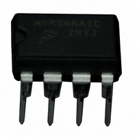
MC9RS08KA1CSC Freescale Semiconductor, MC9RS08KA1CSC Datasheet - Page 20

MC9RS08KA1CSC
Manufacturer Part Number
MC9RS08KA1CSC
Description
IC MCU 8-BIT 1K FLASH 8-SOIC
Manufacturer
Freescale Semiconductor
Series
RS08r
Datasheet
1.DEMO9RS08KA2.pdf
(136 pages)
Specifications of MC9RS08KA1CSC
Core Processor
RS08
Core Size
8-Bit
Speed
10MHz
Peripherals
LVD, POR, WDT
Number Of I /o
4
Program Memory Size
1KB (1K x 8)
Program Memory Type
FLASH
Ram Size
63 x 8
Voltage - Supply (vcc/vdd)
1.8 V ~ 5.5 V
Oscillator Type
Internal
Operating Temperature
-40°C ~ 85°C
Package / Case
8-SOIC (3.9mm Width)
Processor Series
RS08KA
Core
RS08
Data Bus Width
8 bit
Data Ram Size
63 B
Maximum Clock Frequency
20 MHz
Number Of Programmable I/os
4
Operating Supply Voltage
2.7 V to 5.5 V
Maximum Operating Temperature
+ 85 C
Mounting Style
SMD/SMT
Development Tools By Supplier
DEMO9RS08KA8, DEMO9RS08KA2
Minimum Operating Temperature
- 40 C
Lead Free Status / RoHS Status
Lead free / RoHS Compliant
Eeprom Size
-
Data Converters
-
Connectivity
-
Lead Free Status / Rohs Status
Lead free / RoHS Compliant
Available stocks
Company
Part Number
Manufacturer
Quantity
Price
Company:
Part Number:
MC9RS08KA1CSC
Manufacturer:
TI
Quantity:
213
Part Number:
MC9RS08KA1CSC
Manufacturer:
FREESCALE
Quantity:
20 000
Chapter 2 Pins and Connections
cables and the absolute value of the internal pullup device play almost no role in determining rise and fall
times on the BKGD pin.
2.4.4
The remaining pins are shared among general-purpose I/O and on-chip peripheral functions such as timers
and analog comparator. Immediately after reset, all of these pins are configured as high-impedance
general-purpose inputs with internal pullup/pulldown devices disabled.
20
1
2
3
4
5
Pin Name
SWC is software-controlled pullup/pulldown resistor; the register is associated with the respective port.
Alternative functions are listed lowest priority first. For example, GPIO is the lowest priority alternative function of the
PTA0 pin; ACMP+ is the highest priority alternative function of the PTA0 pin.
Output-only when configured as PTA3 function.
When PTA2 or PTA3 is configured as RESET or BKGD/MS, respectively, pullup is enabled. When V
pullup/pulldown is disabled automatically.
This pin is not available in 6-pin package. Enabling either the pullup or pulldown device is recommended to prevent extra
current leakage from the floating input pin.
PTA4
PTA5
PTA0
PTA1
PTA2
PTA3
V
V
DD
SS
5
5
General-Purpose I/O and Peripheral Ports
To avoid extra current drain from floating input pins, the reset initialization
routine in the application program should either enable on-chip
pullup/pulldown devices or change the direction of unused pins to outputs.
Direction
I/O
I/O
I/O
I/O
I/O
—
—
I
3
Pullup/Pulldown
SWC
SWC
SWC
SWC
SWC
—
—
—
MC9RS08KA2 Series Data Sheet, Rev. 4
4
Table 2-1. Pin Sharing Reference
4
1
ACMPO
ACMP+
RESET
ACMP-
KBIP0
KBIP1
KBIP2
BKGD
KBIP4
KBIP5
TCLK
PTA0
PTA1
PTA2
PTA3
PTA4
PTA5
V
NOTE
MS
PP
General-purpose input/output (GPIO)
Keyboard interrupt (stop/wait wakeup only)
Analog comparator input
General-purpose input/output (GPIO)
Keyboard interrupt (stop/wait wakeup only)
Analog comparator input
General-purpose input
Keyboard interrupt (stop/wait wakeup only)
Modulo timer clock source
Reset
V
General-purpose output
Analog comparator output
Background debug data
Mode select
General-purpose input/output (GPIO)
Keyboard interrupt (stop/wait wakeup only)
General-purpose input/output (GPIO)
Keyboard interrupt (stop/wait wakeup only)
PP
Alternative Functions
Ground
Power
2
Freescale Semiconductor
PP
is attached,


