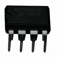
MC9RS08KA1CSC Freescale Semiconductor, MC9RS08KA1CSC Datasheet - Page 45

MC9RS08KA1CSC
Manufacturer Part Number
MC9RS08KA1CSC
Description
IC MCU 8-BIT 1K FLASH 8-SOIC
Manufacturer
Freescale Semiconductor
Series
RS08r
Datasheet
1.DEMO9RS08KA2.pdf
(136 pages)
Specifications of MC9RS08KA1CSC
Core Processor
RS08
Core Size
8-Bit
Speed
10MHz
Peripherals
LVD, POR, WDT
Number Of I /o
4
Program Memory Size
1KB (1K x 8)
Program Memory Type
FLASH
Ram Size
63 x 8
Voltage - Supply (vcc/vdd)
1.8 V ~ 5.5 V
Oscillator Type
Internal
Operating Temperature
-40°C ~ 85°C
Package / Case
8-SOIC (3.9mm Width)
Processor Series
RS08KA
Core
RS08
Data Bus Width
8 bit
Data Ram Size
63 B
Maximum Clock Frequency
20 MHz
Number Of Programmable I/os
4
Operating Supply Voltage
2.7 V to 5.5 V
Maximum Operating Temperature
+ 85 C
Mounting Style
SMD/SMT
Development Tools By Supplier
DEMO9RS08KA8, DEMO9RS08KA2
Minimum Operating Temperature
- 40 C
Lead Free Status / RoHS Status
Lead free / RoHS Compliant
Eeprom Size
-
Data Converters
-
Connectivity
-
Lead Free Status / Rohs Status
Lead free / RoHS Compliant
Available stocks
Company
Part Number
Manufacturer
Quantity
Price
Company:
Part Number:
MC9RS08KA1CSC
Manufacturer:
TI
Quantity:
213
Part Number:
MC9RS08KA1CSC
Manufacturer:
FREESCALE
Quantity:
20 000
Chapter 6
Parallel Input/Output Control
This section explains software controls related to parallel input/output (I/O) and pin control. The
MC9RS08KA2 Series has one parallel I/O port, which includes two I/O pins in the 6-pin package or four
I/O pins in the 8-pin packages, one output-only pin, and one input-only pin. See
Connections,” for more information about pin assignments and external hardware considerations for these
pins.
All of these I/O pins are shared with on-chip peripheral functions as shown in
modules have priority over the I/Os so that when a peripheral is enabled, the I/O functions associated with
the shared pins are disabled. After reset, the shared peripheral functions are disabled so that the pins are
controlled by the I/O. All of the I/Os are configured as inputs (PTADDn = 0) with pullup/pulldown devices
disabled (PTAPEn = 0), except for output-only pin PTA3, which defaults to the BKGD/MS function.
Reading and writing of parallel I/Os is performed through the port data registers. The direction, either input
or output, is controlled through the port data direction registers. The parallel I/O port function for an
individual pin is illustrated in the block diagram shown in
The data direction control bit (PTADDn) determines whether the output buffer for the associated pin is
enabled, and also controls the source for port data register reads. The input buffer for the associated pin is
always enabled unless the pin is enabled as an analog function or is an output-only pin.
Freescale Semiconductor
Port Read
BUSCLK
Data
Figure 6-1. Parallel I/O Block Diagram
MC9RS08KA2 Series Data Sheet, Rev. 4
PTADDn
D
D
PTADn
Q
Q
1
0
Figure
6-1.
Synchronizer
Table
Chapter 2, “Pins and
Output Enable
Output Data
2-1. The peripheral
Input Data
45


