MC908JL8MPE Freescale Semiconductor, MC908JL8MPE Datasheet - Page 187
MC908JL8MPE
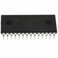
Manufacturer Part Number
MC908JL8MPE
Description
IC MCU 8K FLASH 8MHZ 28-DIP
Manufacturer
Freescale Semiconductor
Series
HC08r
Datasheet
1.MC908JL8CDWER.pdf
(212 pages)
Specifications of MC908JL8MPE
Core Processor
HC08
Core Size
8-Bit
Speed
8MHz
Connectivity
SCI
Peripherals
LED, LVD, POR, PWM
Number Of I /o
15
Program Memory Size
8KB (8K x 8)
Program Memory Type
FLASH
Ram Size
256 x 8
Voltage - Supply (vcc/vdd)
4.5 V ~ 5.5 V
Data Converters
A/D 13x8b
Oscillator Type
Internal
Operating Temperature
-40°C ~ 125°C
Package / Case
28-DIP (0.600", 15.24mm)
Processor Series
HC08JL
Core
HC08
Data Bus Width
8 bit
Data Ram Size
256 B
Interface Type
SCI
Maximum Clock Frequency
8 MHz
Number Of Programmable I/os
23
Number Of Timers
4
Maximum Operating Temperature
+ 125 C
Mounting Style
Through Hole
Development Tools By Supplier
FSICEBASE, DEMO908JL16E, M68CBL05CE
Minimum Operating Temperature
- 40 C
On-chip Adc
13-ch x 8-bit
Controller Family/series
HC08
No. Of I/o's
23
Ram Memory Size
256Byte
Cpu Speed
8MHz
No. Of Timers
2
Embedded Interface Type
SCI, SPI
Rohs Compliant
Yes
Eeprom Size
-
Lead Free Status / Rohs Status
Lead free / RoHS Compliant
Available stocks
Company
Part Number
Manufacturer
Quantity
Price
Company:

Part Number:
MC908JL8MPE
Manufacturer:
Freescale Semiconductor
Quantity:
135


17.5 5V DC Electrical Characteristics
Freescale Semiconductor
Output high voltage (I
Output low voltage (I
Output low voltage (I
LED drives (V
Input high voltage
Input low voltage
V
Digital I/O ports Hi-Z leakage current
Input current
Capacitance
POR rearm voltage
POR rise time ramp rate
Monitor mode entry voltage
Pullup resistors
Low-voltage inhibit, trip falling voltage
Low-voltage inhibit, trip rising voltage
1. V
2. Typical values reflect average measurements at midpoint of voltage range, 25 °C only.
3. Run (operating) I
4. Wait I
5. Stop I
6. Maximum is highest voltage that POR is guaranteed.
7. If minimum V
8. R
DD
PTA0–PTA7, PTB0–PTB7, PTD0–PTD7, PTE0–PTE1
PTA6, PTB0–PTB7, PTD0, PTD1, PTD4, PTD5,
PTD6, PTD7
PTA0–PTA5, PTA7, PTD2, PTD3, PTD6, PTD7
PTA0–PTA7, PTB0–PTB7, PTD0–PTD7, PTE0–PTE1, RST,
PTA0–PTA7, PTB0–PTB7, PTD0–PTD7, PTE0–PTE1, RST,
Run
Wait
Stop
Ports (as input or output)
PTD6, PTD7
RST, IRQ, PTA0–PTA7
XTAL oscillator option
RC oscillator option
XTAL oscillator option
RC oscillator option
XTAL oscillator option
RC oscillator option
PTE0–PTE1
IRQ, OSC1
IRQ, OSC1
Less than 100 pF on all outputs. C
run I
100 pF on all outputs. C
supply current, f
DD
PU1
(3)
(4)
(5)
= 4.5 to 5.5 Vdc, V
DD
(–40°C to 125°C)
DD
and R
DD
. Measured with all modules enabled.
measured using external square wave clock source (f
measured with OSC1 grounded; no port pins sourcing current. LVI is disabled.
OL
DD
(8)
PU2
= 3V)
is not reached before the internal POR reset is released, RST must be driven low externally until minimum V
(6)
are measured at V
DD
MC68HC908JL8/JK8 • MC68HC08JL8/JK8 • MC68HC908KL8 Data Sheet, Rev. 3.1
LOAD
LOAD
OP
LOAD
Characteristic
measured using external square wave clock source (f
= 8MHz
(7)
= 1.6mA)
= 25mA)
= –2.0mA)
SS
L
= 20 pF on OSC2. All ports configured as inputs. OSC2 capacitance linearly affects wait I
= 0 Vdc, T
Table 17-4. DC Electrical Characteristics (5V)
(1)
DD
L
A
= 20 pF on OSC2. All ports configured as inputs. OSC2 capacitance linearly affects
= 5.0V.
= T
L
to T
H
, unless otherwise noted.
Symbol
V
OP
V
C
V
R
R
R
V
V
V
V
TRIPR
TRIPF
V
I
C
I
V
I
POR
I
OUT
POR
OL
DD
TST
PU1
PU2
OH
IN
OL
OL
IL
= 8MHz). All inputs 0.2V from rail. No dc loads. Less than
IH
IL
IN
OP
0.7 × V
1.5 × V
= 8MHz). All inputs 0.2V from rail. No dc loads.
V
DD
0.035
3.60
3.75
Min
V
1.8
10
16
—
—
—
—
—
—
—
—
—
—
—
—
0
SS
–0.8
DD
DD
5V DC Electrical Characteristics
Typ
4.25
4.40
7.5
3.5
1.5
0.5
3.3
16
11
26
—
—
—
—
—
—
—
—
—
—
—
—
3
(2)
0.3 × V
Max
4.48
4.63
V
± 10
100
0.4
0.5
5.5
± 1
8.5
4.8
—
25
10
13
12
—
36
DD
6
8
3
8
DD
DD
is reached.
DD
V/ms
Unit
mA
mA
mA
mA
mA
mV
µA
µA
µA
µA
kΩ
kΩ
pF
.
V
V
V
V
V
V
V
V
187
Related parts for MC908JL8MPE
Image
Part Number
Description
Manufacturer
Datasheet
Request
R

Part Number:
Description:
Manufacturer:
Freescale Semiconductor, Inc
Datasheet:
Part Number:
Description:
Manufacturer:
Freescale Semiconductor, Inc
Datasheet:
Part Number:
Description:
Manufacturer:
Freescale Semiconductor, Inc
Datasheet:
Part Number:
Description:
Manufacturer:
Freescale Semiconductor, Inc
Datasheet:
Part Number:
Description:
Manufacturer:
Freescale Semiconductor, Inc
Datasheet:
Part Number:
Description:
Manufacturer:
Freescale Semiconductor, Inc
Datasheet:
Part Number:
Description:
Manufacturer:
Freescale Semiconductor, Inc
Datasheet:
Part Number:
Description:
Manufacturer:
Freescale Semiconductor, Inc
Datasheet:
Part Number:
Description:
Manufacturer:
Freescale Semiconductor, Inc
Datasheet:
Part Number:
Description:
Manufacturer:
Freescale Semiconductor, Inc
Datasheet:
Part Number:
Description:
Manufacturer:
Freescale Semiconductor, Inc
Datasheet:
Part Number:
Description:
Manufacturer:
Freescale Semiconductor, Inc
Datasheet:
Part Number:
Description:
Manufacturer:
Freescale Semiconductor, Inc
Datasheet:
Part Number:
Description:
Manufacturer:
Freescale Semiconductor, Inc
Datasheet:
Part Number:
Description:
Manufacturer:
Freescale Semiconductor, Inc
Datasheet: