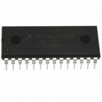
MC908JL8MPE Freescale Semiconductor, MC908JL8MPE Datasheet - Page 85

MC908JL8MPE
Manufacturer Part Number
MC908JL8MPE
Description
IC MCU 8K FLASH 8MHZ 28-DIP
Manufacturer
Freescale Semiconductor
Series
HC08r
Datasheet
1.MC908JL8CDWER.pdf
(212 pages)
Specifications of MC908JL8MPE
Core Processor
HC08
Core Size
8-Bit
Speed
8MHz
Connectivity
SCI
Peripherals
LED, LVD, POR, PWM
Number Of I /o
15
Program Memory Size
8KB (8K x 8)
Program Memory Type
FLASH
Ram Size
256 x 8
Voltage - Supply (vcc/vdd)
4.5 V ~ 5.5 V
Data Converters
A/D 13x8b
Oscillator Type
Internal
Operating Temperature
-40°C ~ 125°C
Package / Case
28-DIP (0.600", 15.24mm)
Processor Series
HC08JL
Core
HC08
Data Bus Width
8 bit
Data Ram Size
256 B
Interface Type
SCI
Maximum Clock Frequency
8 MHz
Number Of Programmable I/os
23
Number Of Timers
4
Maximum Operating Temperature
+ 125 C
Mounting Style
Through Hole
Development Tools By Supplier
FSICEBASE, DEMO908JL16E, M68CBL05CE
Minimum Operating Temperature
- 40 C
On-chip Adc
13-ch x 8-bit
Controller Family/series
HC08
No. Of I/o's
23
Ram Memory Size
256Byte
Cpu Speed
8MHz
No. Of Timers
2
Embedded Interface Type
SCI, SPI
Rohs Compliant
Yes
Eeprom Size
-
Lead Free Status / Rohs Status
Lead free / RoHS Compliant
Available stocks
Company
Part Number
Manufacturer
Quantity
Price
Company:
Part Number:
MC908JL8MPE
Manufacturer:
Freescale Semiconductor
Quantity:
135
- Current page: 85 of 212
- Download datasheet (2Mb)
Chapter 7
Monitor ROM (MON)
7.1 Introduction
This section describes the monitor ROM (MON) and the monitor mode entry methods. The monitor ROM
allows complete testing of the MCU through a single-wire interface with a host computer. This mode is
also used for programming and erasing of FLASH memory in the MCU. Monitor mode entry can be
achieved without use of the higher test voltage, V
blank, thus reducing the hardware requirements for in-circuit programming.
7.2 Features
Features of the monitor ROM include the following:
7.3 Functional Description
The monitor ROM receives and executes commands from a host computer.
circuit used to enter monitor mode and communicate with a host computer via a standard RS-232
interface.
Simple monitor commands can access any memory address. In monitor mode, the MCU can execute
host-computer code in RAM while most MCU pins retain normal operating mode functions. All
communication between the host computer and the MCU is through the PTB0 pin. A level-shifting and
multiplexing interface is required between PTB0 and the host computer. PTB0 is used in a wired-OR
configuration and requires a pull-up resistor.
1. No security feature is absolutely secure. However, Motorola’s strategy is to make reading or copying the FLASH difficult for
Freescale Semiconductor
unauthorized users.
•
•
•
•
•
•
•
•
•
•
Normal user-mode pin functionality
One pin dedicated to serial communication between monitor ROM and host computer
Standard mark/space non-return-to-zero (NRZ) communication with host computer
Execution of code in RAM or FLASH
FLASH memory security feature
FLASH memory programming interface
959 bytes monitor ROM code size
Monitor mode entry without high voltage, V
$FF)
Standard monitor mode entry if high voltage, V
Resident routines for FLASH programming and EEPROM emulation
MC68HC908JL8/JK8 • MC68HC08JL8/JK8 • MC68HC908KL8 Data Sheet, Rev. 3.1
(1)
TST
TST
, as long as vector addresses $FFFE and $FFFF are
, if reset vector is blank ($FFFE and $FFFF contain
TST
, is applied to IRQ
Figure 7-1
shows a example
85
Related parts for MC908JL8MPE
Image
Part Number
Description
Manufacturer
Datasheet
Request
R
Part Number:
Description:
Manufacturer:
Freescale Semiconductor, Inc
Datasheet:
Part Number:
Description:
Manufacturer:
Freescale Semiconductor, Inc
Datasheet:
Part Number:
Description:
Manufacturer:
Freescale Semiconductor, Inc
Datasheet:
Part Number:
Description:
Manufacturer:
Freescale Semiconductor, Inc
Datasheet:
Part Number:
Description:
Manufacturer:
Freescale Semiconductor, Inc
Datasheet:
Part Number:
Description:
Manufacturer:
Freescale Semiconductor, Inc
Datasheet:
Part Number:
Description:
Manufacturer:
Freescale Semiconductor, Inc
Datasheet:
Part Number:
Description:
Manufacturer:
Freescale Semiconductor, Inc
Datasheet:
Part Number:
Description:
Manufacturer:
Freescale Semiconductor, Inc
Datasheet:
Part Number:
Description:
Manufacturer:
Freescale Semiconductor, Inc
Datasheet:
Part Number:
Description:
Manufacturer:
Freescale Semiconductor, Inc
Datasheet:
Part Number:
Description:
Manufacturer:
Freescale Semiconductor, Inc
Datasheet:
Part Number:
Description:
Manufacturer:
Freescale Semiconductor, Inc
Datasheet:
Part Number:
Description:
Manufacturer:
Freescale Semiconductor, Inc
Datasheet:
Part Number:
Description:
Manufacturer:
Freescale Semiconductor, Inc
Datasheet:


