MC9S08RD32PE Freescale Semiconductor, MC9S08RD32PE Datasheet - Page 23
MC9S08RD32PE
Manufacturer Part Number
MC9S08RD32PE
Description
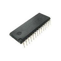
IC MCU 32K FLASH 2K RAM 28-DIP
Manufacturer
Freescale Semiconductor
Series
HCS08r
Datasheet
1.MC9S08RE8FJE.pdf
(234 pages)
Specifications of MC9S08RD32PE
Core Processor
HCS08
Core Size
8-Bit
Speed
8MHz
Connectivity
SCI
Peripherals
LVD, POR, PWM, WDT
Number Of I /o
23
Program Memory Size
32KB (32K x 8)
Program Memory Type
FLASH
Ram Size
2K x 8
Voltage - Supply (vcc/vdd)
1.8 V ~ 3.6 V
Oscillator Type
Internal
Operating Temperature
0°C ~ 70°C
Package / Case
28-DIP (0.600", 15.24mm)
Processor Series
S08RD
Core
HCS08
Data Bus Width
8 bit
Data Ram Size
2 KB
Interface Type
SCI
Maximum Clock Frequency
8 MHz
Number Of Programmable I/os
39
Number Of Timers
2
Operating Supply Voltage
1.8 V to 3.6 V
Maximum Operating Temperature
+ 70 C
Mounting Style
Through Hole
3rd Party Development Tools
EWS08
Development Tools By Supplier
DEMO9S08RG60E
Minimum Operating Temperature
0 C
Lead Free Status / RoHS Status
Lead free / RoHS Compliant
Eeprom Size
-
Data Converters
-
Lead Free Status / Rohs Status
Lead free / RoHS Compliant
Available stocks
Company
Part Number
Manufacturer
Quantity
Price
Company:

Part Number:
MC9S08RD32PE
Manufacturer:
Freescale Semiconductor
Quantity:
135


2.3.1
V
I/O buffer circuitry and to an internal voltage regulator. The internal voltage regulator provides a regulated
lower-voltage source to the CPU and other internal circuitry of the MCU.
Typically, application systems have two separate capacitors across the power pins. In this case, there
should be a bulk electrolytic capacitor, such as a 10-µF tantalum capacitor, to provide bulk charge storage
for the overall system and a 0.1-µF ceramic bypass capacitor located as near to the MCU power pins as
practical to suppress high-frequency noise.
2.3.2
The oscillator in the MC9S08RC/RD/RE/RG is a traditional Pierce oscillator that can accommodate a
crystal or ceramic resonator in the range of 1 MHz to 16 MHz.
Refer to
composition resistor. Wire-wound resistors, and some metal film resistors, have too much inductance. C1
and C2 normally should be high-quality ceramic capacitors specifically designed for high-frequency
applications.
R
value is not generally critical. Typical systems use 1 MΩ. Higher values are sensitive to humidity and lower
values reduce gain and (in extreme cases) could prevent startup.
C1 and C2 are typically in the 5-pF to 25-pF range and are chosen to match the requirements of a specific
crystal or resonator. Be sure to take into account printed circuit board (PCB) capacitance and MCU pin
capacitance when sizing C1 and C2. The crystal manufacturer typically specifies a load capacitance that
is the series combination of C1 and C2, which are usually the same size. As a first-order approximation,
use 5 pF as an estimate of combined pin and PCB capacitance for each oscillator pin (EXTAL and XTAL).
2.3.3
The external pin reset function is shared with an output-only port function on the PTD1/RESET pin. The
reset function is enabled when RSTPE in SOPT is set. RSTPE is set following any reset of the MCU and
must be cleared in order to use this pin as an output-only port.
Whenever any reset is initiated (whether from an external signal or from an internal system), the reset pin
is driven low for about 34 cycles of f
later. If reset was caused by an internal source such as low-voltage reset or watchdog timeout, the circuitry
expects the reset pin sample to return a logic 1. If the pin is still low at this sample point, the reset is
assumed to be from an external source. The reset circuitry decodes the cause of reset and records it by
setting a corresponding bit in the system control reset status register (SRS).
Never connect any significant capacitance to the reset pin because that would interfere with the circuit and
sequence that detects the source of reset. If an external capacitance prevents the reset pin from rising to a
valid logic 1 before the reset sample point, all resets will appear to be external resets.
Freescale Semiconductor
F
DD
is used to provide a bias path to keep the EXTAL input in its linear range during crystal startup and its
and V
Figure 2-5
SS
Power
Oscillator
PTD1/RESET
are the primary power supply pins for the MCU. This voltage source supplies power to all
for the following discussion. R
MC9S08RC/RD/RE/RG Data Sheet, Rev. 1.11
Self_reset
, released, and sampled again about 38 cycles of f
F
should be a low-inductance resistor such as a carbon
Pins and Connections
Self_reset
23
Related parts for MC9S08RD32PE
Image
Part Number
Description
Manufacturer
Datasheet
Request
R

Part Number:
Description:
Manufacturer:
Freescale Semiconductor, Inc
Datasheet:
Part Number:
Description:
Manufacturer:
Freescale Semiconductor, Inc
Datasheet:
Part Number:
Description:
Manufacturer:
Freescale Semiconductor, Inc
Datasheet:
Part Number:
Description:
Manufacturer:
Freescale Semiconductor, Inc
Datasheet:
Part Number:
Description:
Manufacturer:
Freescale Semiconductor, Inc
Datasheet:
Part Number:
Description:
Manufacturer:
Freescale Semiconductor, Inc
Datasheet:
Part Number:
Description:
Manufacturer:
Freescale Semiconductor, Inc
Datasheet:
Part Number:
Description:
Manufacturer:
Freescale Semiconductor, Inc
Datasheet:
Part Number:
Description:
Manufacturer:
Freescale Semiconductor, Inc
Datasheet:
Part Number:
Description:
Manufacturer:
Freescale Semiconductor, Inc
Datasheet:
Part Number:
Description:
Manufacturer:
Freescale Semiconductor, Inc
Datasheet:
Part Number:
Description:
Manufacturer:
Freescale Semiconductor, Inc
Datasheet:
Part Number:
Description:
Manufacturer:
Freescale Semiconductor, Inc
Datasheet:
Part Number:
Description:
Manufacturer:
Freescale Semiconductor, Inc
Datasheet:
Part Number:
Description:
Manufacturer:
Freescale Semiconductor, Inc
Datasheet: