MC908AP32ACFBER Freescale Semiconductor, MC908AP32ACFBER Datasheet - Page 88
MC908AP32ACFBER
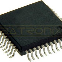
Manufacturer Part Number
MC908AP32ACFBER
Description
IC MCU 32K FLASH 8MHZ 44-QFP
Manufacturer
Freescale Semiconductor
Series
HC08r
Datasheet
1.MC908AP16ACFBER.pdf
(316 pages)
Specifications of MC908AP32ACFBER
Core Processor
HC08
Core Size
8-Bit
Speed
8MHz
Connectivity
I²C, IRSCI, SCI, SPI
Peripherals
LED, LVD, POR, PWM
Number Of I /o
32
Program Memory Size
32KB (32K x 8)
Program Memory Type
FLASH
Ram Size
2K x 8
Voltage - Supply (vcc/vdd)
4.5 V ~ 5.5 V
Data Converters
A/D 8x10b
Oscillator Type
Internal
Operating Temperature
-40°C ~ 85°C
Package / Case
44-QFP
Processor Series
HC08AP
Core
HC08
Data Bus Width
8 bit
Data Ram Size
2 KB
Interface Type
SCI, SPI
Maximum Clock Frequency
8 MHz
Number Of Programmable I/os
32
Number Of Timers
4
Maximum Operating Temperature
+ 85 C
Mounting Style
SMD/SMT
Development Tools By Supplier
FSICEBASE, DEMO908AP64E, M68CBL05CE
Minimum Operating Temperature
- 40 C
On-chip Adc
10 bit, 8 Channel
Lead Free Status / RoHS Status
Lead free / RoHS Compliant
Eeprom Size
-
Lead Free Status / Rohs Status
Details
Available stocks
Company
Part Number
Manufacturer
Quantity
Price
Company:

Part Number:
MC908AP32ACFBER
Manufacturer:
Freescale Semiconductor
Quantity:
10 000


Clock Generator Module (CGM)
6.4.4 Oscillator Output Frequency Signal (CGMXCLK)
CGMXCLK is the oscillator output signal. It runs at the full speed of the oscillator, and is generated directly
from the crystal oscillator circuit, the RC oscillator circuit, or the internal oscillator circuit.
6.4.5 CGM Reference Clock (CGMRCLK)
CGMRCLK is a buffered version of CGMXCLK, this clock is the reference clock for the phase-locked-loop
circuit.
6.4.6 CGM VCO Clock Output (CGMVCLK)
CGMVCLK is the clock output from the VCO.
6.4.7 CGM Base Clock Output (CGMOUT)
CGMOUT is the clock output of the CGM. This signal goes to the SIM, which generates the MCU clocks.
CGMOUT is a 50 percent duty cycle clock running at twice the bus frequency. CGMOUT is software
programmable to be either the oscillator output, CGMXCLK, divided by two or the divided VCO clock,
CGMPCLK, divided by two.
6.4.8 CGM CPU Interrupt (CGMINT)
CGMINT is the interrupt signal generated by the PLL lock detector.
6.5 CGM Registers
The following registers control and monitor operation of the CGM:
88
•
•
•
•
•
PLL control register (PCTL)
(See
PLL bandwidth control register (PBWC)
(See
PLL multiplier select registers (PMSH and PMSL)
(See
PLL VCO range select register (PMRS)
(See
PLL reference divider select register (PMDS)
(See
6.5.1 PLL Control
6.5.2 PLL Bandwidth Control
6.5.3 PLL Multiplier Select
6.5.4 PLL VCO Range Select
6.5.5 PLL Reference Divider Select
Route V
capacitors as close as possible to the package.
SSA
carefully for maximum noise immunity and place bypass
Register.)
MC68HC908AP A-Family Data Sheet, Rev. 3
Registers.)
Register.)
Register.)
Register.)
NOTE
Freescale Semiconductor
Related parts for MC908AP32ACFBER
Image
Part Number
Description
Manufacturer
Datasheet
Request
R

Part Number:
Description:
Manufacturer:
Freescale Semiconductor, Inc
Datasheet:
Part Number:
Description:
Manufacturer:
Freescale Semiconductor, Inc
Datasheet:
Part Number:
Description:
Manufacturer:
Freescale Semiconductor, Inc
Datasheet:
Part Number:
Description:
Manufacturer:
Freescale Semiconductor, Inc
Datasheet:
Part Number:
Description:
Manufacturer:
Freescale Semiconductor, Inc
Datasheet:
Part Number:
Description:
Manufacturer:
Freescale Semiconductor, Inc
Datasheet:
Part Number:
Description:
Manufacturer:
Freescale Semiconductor, Inc
Datasheet:
Part Number:
Description:
Manufacturer:
Freescale Semiconductor, Inc
Datasheet:
Part Number:
Description:
Manufacturer:
Freescale Semiconductor, Inc
Datasheet:
Part Number:
Description:
Manufacturer:
Freescale Semiconductor, Inc
Datasheet:
Part Number:
Description:
Manufacturer:
Freescale Semiconductor, Inc
Datasheet:
Part Number:
Description:
Manufacturer:
Freescale Semiconductor, Inc
Datasheet:
Part Number:
Description:
Manufacturer:
Freescale Semiconductor, Inc
Datasheet:
Part Number:
Description:
Manufacturer:
Freescale Semiconductor, Inc
Datasheet:
Part Number:
Description:
Manufacturer:
Freescale Semiconductor, Inc
Datasheet: