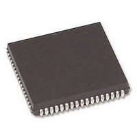
HD6473308RCP10V Renesas Electronics America, HD6473308RCP10V Datasheet - Page 17

HD6473308RCP10V
Manufacturer Part Number
HD6473308RCP10V
Description
MCU 5V 16K,PB-FREE 80-PLCC
Manufacturer
Renesas Electronics America
Series
H8® H8/330r
Datasheet
1.HD6473258P10V.pdf
(349 pages)
Specifications of HD6473308RCP10V
Core Size
8-Bit
Program Memory Size
16KB (16K x 8)
Oscillator Type
Internal
Core Processor
H8/300
Speed
10MHz
Number Of I /o
58
Program Memory Type
OTP
Ram Size
512 x 8
Operating Temperature
-20°C ~ 75°C
Package / Case
80-PLCC
No. Of I/o's
58
Ram Memory Size
512Byte
Cpu Speed
10MHz
No. Of Timers
3
No. Of Pwm Channels
2
Digital Ic Case
RoHS Compliant
Controller Family/series
H8/330
Peripherals
ADC
Rohs Compliant
Yes
Lead Free Status / RoHS Status
Lead free / RoHS Compliant
Voltage - Supply (vcc/vdd)
-
Eeprom Size
-
Data Converters
-
Peripherals
-
Connectivity
-
Lead Free Status / RoHS Status
Lead free / RoHS Compliant
Available stocks
Company
Part Number
Manufacturer
Quantity
Price
Company:
Part Number:
HD6473308RCP10V
Manufacturer:
Renesas Electronics America
Quantity:
10 000
- Current page: 17 of 349
- Download datasheet (2Mb)
Figure 10-1
Figure 10-2
Figure 10-3
Figure 10-4
Figure 10-5
Figure 10-6
Figure 11-1
Figure 11-2
Figure 11-3
Figure 11-4
Figure 12-1
Figure 13-1
Figure 13-2
Figure 13-3
Figure 13-4
Figure 13-5
Figure 13-6
Figure 14-1
Figure 14-2
Figure 15-1
Figure 15-2
Figure 16-1
Figure 16-2
Figure 16-3
Figure 16-4
Figure 16-5
Figure 16-6
Figure 17-1
Figure 17-2
Block Diagram of A/D Converter ......................................................................... 208
The Response of the A/D Converter ..................................................................... 214
A/D Operation in Single Mode (When Channel 1 is Selected)............................. 216
A/D Operation in Scan Mode (When Channel 0 to 2 are Selected)...................... 219
A/D Conversion Timing........................................................................................ 221
External Trigger Input Timing .............................................................................. 222
Block Diagram of Dual-Port RAM ....................................................................... 226
Parallel Communication Data Register 0 .............................................................. 230
Dual-Port RAM Timing Chart .............................................................................. 236
Interconnection to H8/532 (Example)................................................................... 237
Block Diagram of On-Chip RAM......................................................................... 239
Block Diagram of On-Chip ROM......................................................................... 242
Socket Adapter Pin Assignments .......................................................................... 244
Memory Map in PROM Mode .............................................................................. 245
High-Speed Programming Flowchart.................................................................... 246
PROM Write/Verify Timing.................................................................................. 248
Recommended Screening Procedure..................................................................... 249
Software Standby Mode (when) NMI Timing ...................................................... 258
Hardware Standby Mode Timing .......................................................................... 260
Execution Cycle of Instruction Synchronized with E Clock in
Expanded Modes (Maximum Synchronization Delay)......................................... 262
Execution Cycle of Instruction Synchronized with E Clock in
Expanded Modes (Minimum Synchronization Delay).......................................... 263
Block Diagram of Clock Pulse Generator............................................................. 265
Connection of Crystal Oscillator (Example)......................................................... 266
Equivalent Circuit of External Crystal .................................................................. 266
Notes on Board Design around External Crystal .................................................. 267
External Clock Input (Example) ........................................................................... 267
Phase Relationship of System Clock and E Clock................................................ 268
Example of Circuit for Driving a Darlington Pair................................................. 272
Example of Circuit for Driving a LED.................................................................. 272
xiv
Related parts for HD6473308RCP10V
Image
Part Number
Description
Manufacturer
Datasheet
Request
R

Part Number:
Description:
KIT STARTER FOR M16C/29
Manufacturer:
Renesas Electronics America
Datasheet:

Part Number:
Description:
KIT STARTER FOR R8C/2D
Manufacturer:
Renesas Electronics America
Datasheet:

Part Number:
Description:
R0K33062P STARTER KIT
Manufacturer:
Renesas Electronics America
Datasheet:

Part Number:
Description:
KIT STARTER FOR R8C/23 E8A
Manufacturer:
Renesas Electronics America
Datasheet:

Part Number:
Description:
KIT STARTER FOR R8C/25
Manufacturer:
Renesas Electronics America
Datasheet:

Part Number:
Description:
KIT STARTER H8S2456 SHARPE DSPLY
Manufacturer:
Renesas Electronics America
Datasheet:

Part Number:
Description:
KIT STARTER FOR R8C38C
Manufacturer:
Renesas Electronics America
Datasheet:

Part Number:
Description:
KIT STARTER FOR R8C35C
Manufacturer:
Renesas Electronics America
Datasheet:

Part Number:
Description:
KIT STARTER FOR R8CL3AC+LCD APPS
Manufacturer:
Renesas Electronics America
Datasheet:

Part Number:
Description:
KIT STARTER FOR RX610
Manufacturer:
Renesas Electronics America
Datasheet:

Part Number:
Description:
KIT STARTER FOR R32C/118
Manufacturer:
Renesas Electronics America
Datasheet:

Part Number:
Description:
KIT DEV RSK-R8C/26-29
Manufacturer:
Renesas Electronics America
Datasheet:

Part Number:
Description:
KIT STARTER FOR SH7124
Manufacturer:
Renesas Electronics America
Datasheet:

Part Number:
Description:
KIT STARTER FOR H8SX/1622
Manufacturer:
Renesas Electronics America
Datasheet:

Part Number:
Description:
KIT DEV FOR SH7203
Manufacturer:
Renesas Electronics America
Datasheet:


