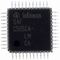
SAF-C515C-8EM CA Infineon Technologies, SAF-C515C-8EM CA Datasheet - Page 45

SAF-C515C-8EM CA
Manufacturer Part Number
SAF-C515C-8EM CA
Description
IC MCU 8BIT OTP MQFP-80-1
Manufacturer
Infineon Technologies
Series
C5xx/C8xxr
Datasheet
1.SAF-C515C-8EM_CA.pdf
(96 pages)
Specifications of SAF-C515C-8EM CA
Core Processor
C500
Core Size
8-Bit
Speed
10MHz
Connectivity
CAN, EBI/EMI, SPI, UART/USART
Peripherals
POR, PWM, WDT
Number Of I /o
49
Program Memory Size
64KB (64K x 8)
Program Memory Type
OTP
Ram Size
2.5K x 8
Voltage - Supply (vcc/vdd)
4.25 V ~ 5.5 V
Data Converters
A/D 8x10b
Oscillator Type
External
Operating Temperature
-40°C ~ 85°C
Package / Case
80-SQFP
Data Bus Width
8 bit
Data Ram Size
2.25 KB
Interface Type
USART, SSC
Maximum Clock Frequency
10 MHz
Number Of Programmable I/os
49
Number Of Timers
3
Operating Supply Voltage
5 V
Maximum Operating Temperature
+ 85 C
Mounting Style
SMD/SMT
Minimum Operating Temperature
- 40 C
On-chip Adc
10 bit, 8 Channel
Packages
PG-MQFP-80
Max Clock Frequency
10.0 MHz
Sram (incl. Cache)
2.25 KByte
Can Nodes
1
A / D Input Lines (incl. Fadc)
8
Program Memory
64.0 KByte
Lead Free Status / RoHS Status
Lead free / RoHS Compliant
Eeprom Size
-
Lead Free Status / Rohs Status
Details
Other names
F515C8EMCANP
F515C8EMCAXT
SAF-C515C-8EMCA
SAF-C515C-8EMCA
SAF-C515C-8EMCAIN
SAFC515C8EMCAX
SP000068749
SP000106399
F515C8EMCAXT
SAF-C515C-8EMCA
SAF-C515C-8EMCA
SAF-C515C-8EMCAIN
SAFC515C8EMCAX
SP000068749
SP000106399
SSC Interface
The C515C microcontroller provides a Synchronous Serial Channel unit, the SSC. This
interface is compatible to the popular SPI serial bus interface.
diagram of the SSC. The central element of the SSC is an 8-bit shift register. The input
and the output of this shift register are each connected via a control logic to the pin P4.2
/ SRI (SSC Receiver In) and P4.3 / STO (SSC Transmitter Out). This shift register can
be written to (SFR STB) and can be read through the Receive Buffer Register SRB.
Figure 16
The SSC has implemented a clock control circuit, which can generate the clock via a
baud rate generator in the master mode, or receive the transfer clock in the slave mode.
The clock signal is fully programmable for clock polarity and phase. The pin used for the
clock signal is P4.1 / SCLK. When operating in slave mode, a slave select input is
provided which enables the SSC interface and also will control the transmitter output.
The pin used for this is P4.4 / SLS.
The SSC control block is responsible for controlling the different modes and operation of
the SSC, checking the status, and generating the respective status and interrupt signals.
Data Sheet
Clock Divider
Control Register
Int. Enable Reg.
Clock Selection
f
OSC
SSC Block Diagram
SSCCON
Interrupt
SCIEN
Status Register
Control Logic
Receive Buffer Register
SCF
Shift Register
41
SRB
STB
Internal Bus
Figure 16
Control
Logic
Pin
shows the block
P4.1/SCLK
P4.2/SRI
P4.3/STO
P4.4/SLS
MCB02735
C515C
2003-02


