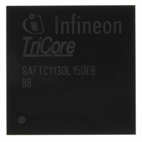
SAF-TC1130-L150EB-G BB Infineon Technologies, SAF-TC1130-L150EB-G BB Datasheet - Page 73

SAF-TC1130-L150EB-G BB
Manufacturer Part Number
SAF-TC1130-L150EB-G BB
Description
IC MCU 32BIT TRICOR 16KB LBGA208
Manufacturer
Infineon Technologies
Series
TC11xxr
Datasheet
1.SAF-TC1130-L100EB-G_BB.pdf
(114 pages)
Specifications of SAF-TC1130-L150EB-G BB
Core Processor
TriCore
Core Size
32-Bit
Speed
150MHz
Connectivity
CAN, EBI/EMI, FIFO, I²C, IrDA, SPI, UART/USART, USB
Peripherals
DMA, POR, PWM, WDT
Number Of I /o
72
Program Memory Type
ROMless
Ram Size
144K x 8
Voltage - Supply (vcc/vdd)
1.43 V ~ 1.58 V
Oscillator Type
External
Operating Temperature
-40°C ~ 85°C
Package / Case
208-LSBGA
Data Bus Width
32 bit
Program Memory Size
32 KB
Data Ram Size
144 KB
Interface Type
3xASC, 2xSSC, I2C, 2xMLI, Ethernet 10, 100 Mbits, s, USB
Maximum Clock Frequency
150 MHz
Number Of Programmable I/os
72
Number Of Timers
9
Operating Supply Voltage
1.5 V, 3.3 V
Maximum Operating Temperature
+ 85 C
Mounting Style
SMD/SMT
Minimum Operating Temperature
- 40 C
Packages
PG-LBGA-208
Max Clock Frequency
150.0 MHz
Sram (incl. Cache)
144.0 KByte
Can Nodes
4
Program Memory
0.0 KByte
Lead Free Status / RoHS Status
Lead free / RoHS Compliant
Eeprom Size
-
Program Memory Size
-
Data Converters
-
Lead Free Status / Rohs Status
Details
Other names
FT1130L150EBGBBXP
SAF-TC1130-L150EB-GBB
SAF-TC1130-L150EB-GBBINTR
SAF-TC1130-L150EB-GBBTR
SAF-TC1130-L150EB-GBBTR
SAFTC1130L150EBBBXT
SP000106119
SP000106538
SP000743584
SAF-TC1130-L150EB-GBB
SAF-TC1130-L150EB-GBBINTR
SAF-TC1130-L150EB-GBBTR
SAF-TC1130-L150EB-GBBTR
SAFTC1130L150EBBBXT
SP000106119
SP000106538
SP000743584
3.24
The Clock Generation Unit (CGU) allows a flexible clock generation for TC1130. The
power consumption is indirectly proportional to the frequency, whereas the performance
of the microcontroller is directly proportional to the frequency. During user program
execution, the frequency can be programmed for an optimal ratio between performance
and power consumption. Therefore, the power consumption can be adapted to the actual
application state.
Features:
The Clock Generation Unit serves several purposes:
• PLL feature for multiplying clock source by different factors
• Direct Drive for direct clock input
• Comfortable state machine for secure switching between basic PLL, direct, or
• Sleep and Power-down mode support
• USB Clock source and control
The Clock Generation Unit in the TC1130, shown in
circuit and one Phase-Locked Loop (PLL). The PLL can convert a low-frequency
external clock signal to a high-speed internal clock for maximum performance. The PLL
also has fail-safe logic that detects degenerate external clock behavior such as abnormal
frequency deviations or a total loss of the external clock. It can execute emergency
actions if it looses the lock on the external clock.
In general, the Clock Generation Unit (CGU) is controlled through the System Control
Unit (SCU) module of the TC1130.
Figure 3-16 Clock Generation Unit Block Diagram
Data Sheet
prescaler operation
XTAL1
XTAL2
Clock G eneration Unit
CG U
System Control Unit
SCU
OGC
Register OSC_CON
Oscillator
Circuit
Clock Generation Unit
MOSC
Detect.
OSCR
Osc.
f
Run
OSC
PDIV
[2:0]
Divi-
der
P
OSC
DISC
>
1
Detector
PLL_
LOCK
Lock
PLL
Detect.
Phase
Divider
NDIV
[6:0]
Register PLL_CLC
N
67
VCO
VCO_
SEL[1:0]
f
VCO
Figure
VCO_
BYPASS
1
0
MUX
KDIV
[3:0]
3-16, consists of an oscillator
Divider
K:1/K:2
Divider
1:1/1:2
SYS
FSL
Functional Description
PLL_
BYPASS
MUX
Register SCU_CON
Divider
USBC
LDIV
V1.1, 2008-12
M CA 04940m od
USBCLK
USBC
LSEL
MUX
TC1130
f
f
SYS
CPU
P4.0/
f
USB


