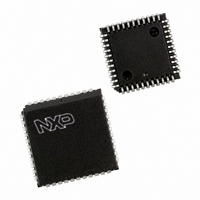
PXAG37KBA,512 NXP Semiconductors, PXAG37KBA,512 Datasheet - Page 6

PXAG37KBA,512
Manufacturer Part Number
PXAG37KBA,512
Description
IC XA MCU 16BIT 32K OTP 44-PLCC
Manufacturer
NXP Semiconductors
Series
XAr
Datasheet
1.PXAG37KFA512.pdf
(37 pages)
Specifications of PXAG37KBA,512
Core Processor
XA
Core Size
16-Bit
Speed
30MHz
Connectivity
UART/USART
Peripherals
PWM, WDT
Number Of I /o
32
Program Memory Size
32KB (32K x 8)
Program Memory Type
OTP
Ram Size
512 x 8
Voltage - Supply (vcc/vdd)
2.7 V ~ 5.5 V
Oscillator Type
External
Operating Temperature
0°C ~ 70°C
Package / Case
44-PLCC
Lead Free Status / RoHS Status
Lead free / RoHS Compliant
Eeprom Size
-
Data Converters
-
Other names
568-1095-5
935263501512
PXAG37KBA
935263501512
PXAG37KBA
Available stocks
Company
Part Number
Manufacturer
Quantity
Price
Company:
Part Number:
PXAG37KBA,512
Manufacturer:
NXP Semiconductors
Quantity:
10 000
Philips Semiconductors
PIN DESCRIPTIONS
2002 Mar 25
MNEMONIC
MNEMONIC
P0.0 – P0.7
P1.0 – P1.7
P2.0 – P2.7
P3.0 – P3.7
ALE/PROG
XA 16-bit microcontroller family
32K OTP, 512 B RAM, watchdog, 2 UARTs
RST
V
V
SS
DD
PLCC
23, 44
43–36
24–31
13–19
1, 22
2–9
11,
13
14
15
16
17
18
19
10
33
11
2
3
4
5
6
7
8
9
PIN. NO.
40–44,
37–30
18–25
LQFP
7–13
1–3
16
17
40
41
42
43
44
10
12
13
27
11
5,
1
2
3
5
7
8
9
4
TYPE
TYPE
I/O
I/O
I/O
I/O
I/O
I/O
I/O
I/O
O
O
O
O
O
O
O
O
I
I
I
I
I
I
I
I
Ground: 0 V reference.
Power Supply: This is the power supply voltage for normal, idle, and power down operation.
Port 0: Port 0 is an 8-bit I/O port with a user-configurable output type. Port 0 latches have 1s
written to them and are configured in the quasi-bidirectional mode during reset. The operation of
port 0 pins as inputs and outputs depends upon the port configuration selected. Each port pin is
configured independently. Refer to the section on I/O port configuration and the DC Electrical
Characteristics for details.
When the external program/data bus is used, Port 0 becomes the multiplexed low data/instruction
byte and address lines 4 through 11.
Port 1: Port 1 is an 8-bit I/O port with a user-configurable output type. Port 1 latches have 1s
written to them and are configured in the quasi-bidirectional mode during reset. The operation of
port 1 pins as inputs and outputs depends upon the port configuration selected. Each port pin is
configured independently. Refer to the section on I/O port configuration and the DC Electrical
Characteristics for details.
Port 1 also provides special functions as described below.
Port 2: Port 2 is an 8-bit I/O port with a user-configurable output type. Port 2 latches have 1s
written to them and are configured in the quasi-bidirectional mode during reset. The operation of
port 2 pins as inputs and outputs depends upon the port configuration selected. Each port pin is
configured independently. Refer to the section on I/O port configuration and the DC Electrical
Characteristics for details.
When the external program/data bus is used in 16-bit mode, Port 2 becomes the multiplexed high
data/instruction byte and address lines 12 through 19. When the external program/data bus is used in
8-bit mode, the number of address lines that appear on port 2 is user programmable.
Port 3: Port 3 is an 8-bit I/O port with a user configurable output type. Port 3 latches have 1s
written to them and are configured in the quasi-bidirectional mode during reset. the operation of
port 3 pins as inputs and outputs depends upon the port configuration selected. Each port pin is
configured independently. Refer to the section on I/O port configuration and the DC Electrical
Characteristics for details.
Port 3 also provides various special functions as described below.
Reset: A low on this pin resets the microcontroller, causing I/O ports and peripherals to take on
their default states, and the processor to begin execution at the address contained in the reset
vector. Refer to the section on Reset for details.
Address Latch Enable/Program Pulse: A high output on the ALE pin signals external circuitry to
latch the address portion of the multiplexed address/data bus. A pulse on ALE occurs only when it
is needed in order to process a bus cycle.
A0/WRH:
A1:
A2:
A3:
RxD1 (P1.4):
TxD1 (P1.5):
T2 (P1.6):
T2EX (P1.7):
RxD0 (P3.0):
TxD0 (P3.1):
INT0 (P3.2):
INT1 (P3.3):
T0 (P3.4):
T1/BUSW (P3.5):
WRL (P3.6):
RD (P3.7):
Address bit 0 of the external address bus when the external data bus is
configured for an 8 bit width. When the external data bus is configured for a 16
bit width, this pin becomes the high byte write strobe.
Address bit 1 of the external address bus.
Address bit 2 of the external address bus.
Address bit 3 of the external address bus.
Receiver input for serial port 1.
Transmitter output for serial port 1.
Timer/counter 2 external count input/clockout.
Timer/counter 2 reload/capture/direction control
Receiver input for serial port 0.
Transmitter output for serial port 0.
External interrupt 0 input.
External interrupt 1 input.
Timer 0 external input, or timer 0 overflow output.
Timer 1 external input, or timer 1 overflow output. The value on this pin is
latched as the external reset input is released and defines the default
external data bus width (BUSW). 0 = 8-bit bus and 1 = 16-bit bus.
External data memory low byte write strobe.
External data memory read strobe.
4
NAME AND FUNCTION
NAME AND FUNCTION
XA-G37
Product data


