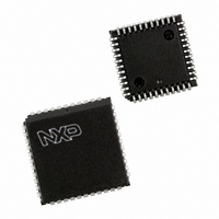
PXAC37KFA/00,512 NXP Semiconductors, PXAC37KFA/00,512 Datasheet - Page 15

PXAC37KFA/00,512
Manufacturer Part Number
PXAC37KFA/00,512
Description
IC XA MCU 16BIT 32K OTP 44-PLCC
Manufacturer
NXP Semiconductors
Series
XAr
Datasheet
1.PXAC37KFA00512.pdf
(68 pages)
Specifications of PXAC37KFA/00,512
Core Processor
XA
Core Size
16-Bit
Speed
32MHz
Connectivity
CAN, EBI/EMI, SPI, UART/USART
Peripherals
DMA, POR, PWM, WDT
Number Of I /o
32
Program Memory Size
32KB (32K x 8)
Program Memory Type
OTP
Ram Size
1K x 8
Voltage - Supply (vcc/vdd)
4.5 V ~ 5.5 V
Oscillator Type
External
Operating Temperature
-40°C ~ 85°C
Package / Case
44-PLCC
Lead Free Status / RoHS Status
Lead free / RoHS Compliant
Eeprom Size
-
Data Converters
-
Other names
568-3533-5
935266516512
PXAC37KFA
935266516512
PXAC37KFA
Available stocks
Company
Part Number
Manufacturer
Quantity
Price
Company:
Part Number:
PXAC37KFA/00,512
Manufacturer:
NXP Semiconductors
Quantity:
10 000
1. All active–low signals are indicated by a “/” symbol.
Philips Semiconductors
NOTE:
2000 Jan 25
ALE ; PROG/
XA 16-bit microcontroller family
32K/1024 OTP CAN transport layer controller
1 UART, 1 SPI Port, CAN 2.0B, 32 CAN ID filters, transport layer co-processor
MNEMONIC
EA/ ; WAIT ;
CAN RxD
CAN TxD
PSEN/
XTAL1
XTAL2
RST/
P3.4
P3.5
P3.6
P3.7
V
PP
PLCC
PIN NUMBERS
16
17
18
19
10
33
32
35
12
34
21
20
LQFP
10
11
12
13
27
26
29
28
15
14
4
6
TYPE
I/O
I/O
I/O
O
O
O
O
O
I
I
I
I
T0: Timer 0 External count input or Timer 0 Overflow output.
T1 : Timer 1 External count input or Timer 1 Overflow output.
WRL/: External DATA memory Low Byte Write Strobe.
RD/: External DATA memory Read Strobe.
RESET/:
NOTE:
10. A low on this pin resets the XA–C3, causing I/O Ports and peripherals to take on
Refer to the Reset section for details.
Address Latch Enable ; Program Pulse/:
NOTES:
11. A high output on the ALE pin signals External circuitry to latch the address portion of
12. A pulse on ALE occurs only when needed to process an External bus cycle. During
Program Store Enable/:
This is the Read Strobe for External PROGRAM memory.
NOTES:
13. When the microcontroller accesses External PROGRAM memory, PSEN/ is driven
14. PSEN/ is only active when External code accesses are performed.
External Access/ ; WAIT ; Programming Supply Voltage:
NOTES:
15. The EA/ input determines whether the internal PROGRAM memory of the XA–C3 is
16. The EA/ pin is latched as the (External) Reset input is released and its value applied
17. After Reset is released, this pin takes on the function of a Bus WAIT input. If WAIT
18. During EPROM programming, this pin is also the programming supply voltage input.
CAN Receive Data input: CAN serial receiver input to the SJA1000 PeliCAN core.
CAN Transmit Data output: CAN serial transmitter output from the SJA1000 PeliCAN
core.
Crystal 1: Input to the inverting amplifier used in the oscillator circuit and input to the
internal clock generator circuits.
Crystal 2: Output from the oscillator amplifier.
their default states, and the processor to begin execution at the Address contained in
the Reset Vector.
the multiplexed Address/DATA bus.
EPROM programming, this pin is used as the Program pulse input.
low in order to enable memory devices.
used for code execution.
during later execution. When latched as a 0, External PROGRAM memory is used
exclusively. When latched as a 1, internal PROGRAM memory will be used up to its
limit, and External PROGRAM memory is used above that point.
is asserted High during any External bus access, that cycle will be extended until
WAIT is released.
8
NAME AND FUNCTION
Preliminary specification
XA-C3


