Z8F3201VN020EC00TR Zilog, Z8F3201VN020EC00TR Datasheet
Z8F3201VN020EC00TR
Specifications of Z8F3201VN020EC00TR
Available stocks


Related parts for Z8F3201VN020EC00TR


Z8F3201VN020EC00TR Summary of contents
Page 1
... Z8F640x, Z8F480x, Z8F320x, Z8F240x, and Z8F160x Z8 Encore! with Flash Memory and 10-Bit A/D Converter Product Specification PS017610-0404 ZiLOG Worldwide Headquarters • 532 Race Street • San Jose, CA 95126-3432 Telephone: 408.558.8500 • Fax: 408.558.8300 • Microcontrollers ™ www.ZiLOG.com ...
Page 2
... Fax: 408.558.8300 www.ZiLOG.com Document Disclaimer ZiLOG is a registered trademark of ZiLOG Inc. in the United States and in other countries. All other products and/or service names mentioned herein may be trademarks of the companies with which they are associated. ©2004 by ZiLOG, Inc. All rights reserved. Information in this publication concerning the devices, applications, or technology described is intended to suggest possible uses and may be superseded ...
Page 3
Table of Contents Introduction . . . . . . . . . . . . . . . . . . . . . . . . . . . . . . . . . . . . ...
Page 4
External Pin Reset . . . . . . . . . . . . . . . . . . . . . . . . . . . . . . . . . . . . . ...
Page 5
Timer Operating Modes . . . . . . . . . . . . . . . . . . . . . . . . . . . . . . . . . 58 Reading the Timer ...
Page 6
Transmitting IrDA Data . . . . . . . . . . . . . . . . . . . . . . . . . . . . . . . . . 96 Receiving IrDA Data ...
Page 7
DMA_ADC Operation . . . . . . . . . . . . . . . . . . . . . . . . . . . . . . . . . 123 Configuring DMA_ADC for Data ...
Page 8
Option Bits . . . . . . . . . . . . . . . . . . . . . . . . . . . . . . . . . . . . . . ...
Page 9
Assembly Language Syntax . . . . . . . . . . . . . . . . . . . . . . . . . . . . . . . . 183 eZ8 CPU Instruction Notation ...
Page 10
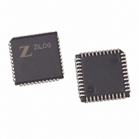
List of Figures Figure 1. Z8 Encore! Figure 2. Z8Fxx01 in 40-Pin Dual Inline Package (DIP Figure 3. Z8Fxx01 in 44-Pin Plastic Leaded Chip Carrier (PLCC ...
Page 11
Figure 31. Flash Controller Operation Flow Chart . . . . . . . . . . . . . . 140 Figure 32. On-Chip Debugger Block Diagram . . . . . . . . . . . . ...
Page 12
List of Tables Table 1. Z8F640x Family Part Selection Guide . . . . . . . . . . . . . . . . 2 Table 2. Z8F640x Family Package Options . . . . . . . ...
Page 13
Table 32. IRQ2 Enable and Priority Encoding . . . . . . . . . . . . . . . . . 53 Table 33. IRQ1 Enable High Bit Register (IRQ1ENH ...
Page 14
Table 67. I2C Data Register (I2CDATA 118 Table 68. I2C Status Register (I2CSTAT ...
Page 15
Table 101. Absolute Maximum Ratings . . . . . . . . . . . . . . . . . . . . . . 167 Table 102. DC Characteristics . . . . . . . . ...
Page 16
... Therefore, we have designed this Product Specification to be used either as a how to procedural manual or a reference guide to important data. Intended Audience This document is written for ZiLOG customers who are experienced at working with microcontrollers, integrated circuits, or printed circuit assemblies. Manual Conventions The following assumptions and conventions are adopted to provide clarity and ease of use: ...
Page 17
Braces The curly braces indicate a single register or bus created by concatenating some com- bination of smaller registers, buses, or individual bits. • Example: the 12-bit register address { hexadecimal value ( (RP) and Working Register R1. ...
Page 18
... It is important that all users understand the following safety terms, which are defined here. Caution: Indicates a procedure or file may become corrupted if the user does not fol- low directions. Trademarks ZiLOG, eZ8, Z8 Encore!, and Z8 are trademarks of countries. All other trademarks are the property of their respective corporations. PS017610-0404 Z8F640x/Z8F480x/Z8F320x/Z8F240x/Z8F160x ZiLOG, Inc. ...
Page 19
... Two Infrared Data Association (IrDA)-compliant infrared encoder/decoder with the UARTs • Watch-Dog Timer (WDT) with internal RC oscillator • I/O pins • Voltage Brown-out Protection (VBO) PS017610-0404 Z8F640x/Z8F480x/Z8F320x/Z8F240x/Z8F160x MCU family of products are the first in a line of ZiLOG microcontroller ® Z8 Encore! 1 ® or the Z8F640x fam- s integrated Introduction ...
Page 20
Power-On Reset (POR) • 3.0-3.6V operating voltage with 5V-tolerant inputs • 0° to +70°C standard temperature and -40° to +105°C extended temperature operating ranges Part Selection Guide Table 1 identifies the basic features and package styles available for each ...
Page 21
... CPU and Peripheral Overview eZ8 CPU Features The eZ8, ZiLOG’s latest 8-bit Central Processing Unit (CPU), meets the continuing demand for faster and more code-efficient microcontrollers. The eZ8 CPU executes a superset of the original Z8 instruction set. The eZ8 CPU features include: • ...
Page 22
... C-Compiler friendly • 2-9 clock cycles per instruction For more information regarding the eZ8 CPU, refer to the eZ8 CPU User Manual avail- able for download at www.zilog.com. General Purpose I/O ® The Z8 Encore! general purpose I/O (GPIO). Each pin is individually programmable. ...
Page 23
Serial Peripheral Interface The serial peripheral interface (SPI) allows the Z8 Encore! other peripheral devices such as EEPROMs, A/D converters and ISDN devices. The SPI is a full-duplex, synchronous, character-oriented channel that supports a four-wire interface. Timers Up to four ...
Page 24
Signal and Pin Descriptions Overview The Z8F640x family products are available in a variety of packages styles and pin config- urations. This chapter describes the signals and available pin configurations for each of the package styles. For information regarding the ...
Page 25
Pin Configurations Figures 56 through 61 illustrate the pin configurations for all of the packages available in ® the Z8 Encore! PD4/RXD1 PC5 / MISO PA3 / CTS0 PA1 / T0OUT PA0 / T0IN PC2 / SS PB0 / ANA0 ...
Page 26
PA0 / T0IN PD2 PC2 / SS RESET VDD VSS PD1 PD0 XOUT XIN VDD Note: Timer 3 is not supported. Figure 57. Z8Fxx01 in 44-Pin Plastic Leaded Chip Carrier (PLCC) PS017610-0404 Z8F640x/Z8F480x/Z8F320x/Z8F240x/Z8F160x ...
Page 27
PA0 / T0IN PD2 PC2 / SS RESET VDD VSS PD1 PD0 XOUT XIN VDD Note: Timer 3 is not supported. Figure 58. Z8Fxx01 in 44-Pin Low-Profile Quad Flat Package (LQFP) PS017610-0404 Z8F640x/Z8F480x/Z8F320x/Z8F240x/Z8F160x ...
Page 28
PA0 / T0IN 49 PD2 PC2 / SS RESET VDD PE4 PE3 VSS 56 PE2 PE1 PE0 VSS PD1 / T3OUT PD0 / T3IN XOUT 64 XIN 1 Figure 59. Z8Fxx02 in 64-Pin Low-Profile Quad Flat Package (LQFP) PS017610-0404 ...
Page 29
PA0 / T0IN 10 PD2 PC2 / SS RESET VDD PE4 PE3 VSS 18 PE2 PE1 PE0 VSS VDD PD1 / T3OUT PD0 / T3IN XOUT XIN 26 27 Figure 60. Z8Fxx02 in 68-Pin Plastic Leaded Chip Carrier (PLCC) ...
Page 30
PA0 / T0IN 1 PD2 PC2 / SS PF6 RESET 5 VDD PF5 PF4 PF3 10 PE4 PE3 VSS PE2 PE1 15 PE0 VSS PF2 PF1 PF0 20 VDD PD1 / T3OUT PD0 / T3IN XOUT XIN 24 25 ...
Page 31
Signal Descriptions Table 2 describes the Z8F640x family signals. Refer to the section Pin Configurations on page 7 to determine the signals available for the specific package styles. Table 2. Signal Descriptions Signal Mnemonic I/O Description General-Purpose I/O Ports A-H ...
Page 32
Table 2. Signal Descriptions (Continued) Signal Mnemonic I/O Description UART Controllers TXD0 / TXD1 O Transmit Data. These signals are the transmit outputs from the UARTs. The TXD signals are multiplexed with general-purpose I/O pins. RXD0 / RXD1 I Receive ...
Page 33
Table 2. Signal Descriptions (Continued) Signal Mnemonic I/O Description Reset RESET I RESET. Generates a Reset when asserted (driven Low). Power Supply VDD I Power Supply. AVDD I Analog Power Supply. VSS I Ground. AVSS I Analog Ground. Pin Characteristics ...
Page 34
Table 3. Pin Characteristics of the Symbol Reset Mnemonic Direction Direction PF[7:0] I/O I PG[7:0] I/O I PH[3:0] I/O I RESET I I VDD N/A N/A XIN I I XOUT represents integer 0, 1,... to indicate multiple ...
Page 35
... These three address spaces are covered briefly in the following subsections. For more detailed information regarding the eZ8 CPU and its address space, refer to the eZ8 CPU User Manual available for download at www.zilog.com. Register File The Register File address space in the Z8 Encore! is composed of two sections— ...
Page 36
Program Memory The eZ8 CPU supports 64KB of Program Memory address space. The Z8F640x family devices contain 16KB to 64KB of on-chip Flash memory in the Program Memory address space. Reading from Program Memory addresses outside the available Flash memory ...
Page 37
Table 4. Z8F640x Family Program Memory Maps (Continued) Program Memory Address (Hex) Z8F480x Products 0000-0001 0002-0003 0004-0005 0006-0007 0008-0037 0038-BFFFH Z8F640x Products 0000-0001 0002-0003 0004-0005 0006-0007 0008-0037 0038-FFFFH * See Table 22 on page 45 for a list of the ...
Page 38
Register File Address Map Table 6 provides the address map for the Register File of the Z8F640x family of products. Not all devices and package styles in the Z8F640x family support Timer 3 and all of the GPIO Ports. Consider ...
Page 39
Table 6. Register File Address Map (Continued) Address (Hex) Register Description Timer 3 (not available in 40- and 44- Pin Packages) F18 Timer 3 High Byte F19 Timer 3 Low Byte F1A Timer 3 Reload High Byte F1B Timer 3 ...
Page 40
Table 6. Register File Address Map (Continued) Address (Hex) Register Description F62 SPI Status F63 SPI Mode F64-F65 Reserved F66 SPI Baud Rate High Byte F67 SPI Baud Rate Low Byte F68-F69 Reserved Analog-to-Digital Converter (ADC) F70 ADC Control F71 ...
Page 41
Table 6. Register File Address Map (Continued) Address (Hex) Register Description FCE Interrupt Port Select FCF Interrupt Control GPIO Port A FD0 Port A Address FD1 Port A Control FD2 Port A Input Data FD3 Port A Output Data GPIO ...
Page 42
Table 6. Register File Address Map (Continued) Address (Hex) Register Description FED Port H Control FEE Port H Input Data FEF Port H Output Data Watch-Dog Timer (WDT) FF0 Watch-Dog Timer Control FF1 Watch-Dog Timer Reload Upper Byte FF2 Watch-Dog ...
Page 43
Reset and Stop Mode Recovery Overview The Reset Controller within the Z8F640x family devices controls Reset and STOP Mode Recovery operation. In typical operation, the following events cause a Reset to occur: • Power-On Reset (POR) • Voltage Brown-Out (VBO) ...
Page 44
System and Short Resets During a System Reset, the Z8F640x family device is held in Reset for 514 cycles of the Watch-Dog Timer oscillator followed by 16 cycles of the system clock (crystal oscillator). A Short Reset differs from a ...
Page 45
Power-On Reset The Z8F640x family products contain an internal Power-On Reset (POR) circuit. The POR circuit monitors the supply voltage and holds the device in the Reset state until the supply voltage reaches a safe operating level. After the supply ...
Page 46
V age remains below the Power-On Reset voltage threshold (V the Z8F640x family device in the Reset state. After the supply voltage again exceeds the Power-On Reset voltage threshold, the Z8F640x family device progresses through a full System ...
Page 47
External Pin Reset The RESET pin has a Schmitt-triggered input and an internal pull-up. Once the RESET pin is asserted, the device progresses through the Short Reset sequence. While the RESET input pin is asserted Low, the Z8F640x family device ...
Page 48
Stop Mode Recovery Using a GPIO Port Pin Transition Each of the GPIO Port pins may be configured as a Stop Mode Recovery input source. On any GPIO pin enabled as a Stop Mode Recover source, a change in the ...
Page 49
Low-Power Modes Overview The Z8F640x family products contain power-saving features. The highest level of power reduction is provided by Stop mode. The next level of power reduction is provided by the Halt mode. Stop Mode Execution of the eZ8 CPU’s ...
Page 50
Watch-Dog Timer’s internal RC oscillator continues to operate • If enabled, the Watch-Dog Timer continues to operate • All other on-chip peripherals continue to operate The eZ8 CPU can be brought out of Halt mode by any of the ...
Page 51
General-Purpose I/O Overview The Z8F640x family products support a maximum of seven 8-bit ports (Ports A-G) and one 4-bit port (Port H) for general-purpose input/output (I/O) operations. Each port con- tains control and data registers. The GPIO control registers are ...
Page 52
Table 10. Port Availability by Device and Package Type (Continued) Device Packages Port A Z8F6401 44-pin [7:0] Z8F6402 64- and 68-pin [7:0] Z8F6403 80-pin [7:0] Architecture Figure 64 illustrates a simplified block diagram of a GPIO port pin. In this ...
Page 53
Port A-H Data Direction regis- ters to the alternate function assigned to this pin. Table 11 lists the alternate functions asso- ciated with each port pin. Table 11. Port Alternate ...
Page 54
Table 11. Port Alternate Function Mapping (Continued) Port Pin Port D PD0 PD1 PD2 PD3 PD4 PD5 PD6 PD7 Port E PE[7:0] N/A Port F PF[7:0] N/A Port G PG[7:0] N/A Port H PH0 PH1 PH2 PH3 GPIO Interrupts Many ...
Page 55
Table 12. GPIO Port Registers and Sub-Registers Port Register Mnemonic PxADDR PxCTL PxIN PxOUT Port Sub-Register Mnemonic PxDD PxAF PxOC PxHDE PxSMRE Port A-H Address Registers The Port A-H Address registers select the GPIO Port functionality accessible through the Port ...
Page 56
PADDR[7:0]—Port Address The Port Address selects one of the sub-registers accessible through the Port Control reg- ister. PADDR[7:0] 00H 01H 02H 03H 04H 05H 06H-FFH Port A-H Control Registers The Port A-H Control registers set the GPIO port operation. The ...
Page 57
Port A-H Data Direction Sub-Registers The Port A-H Data Direction sub-register is accessed through the Port A-H Control regis- ter by writing 01H to the Port A-H Address register (Table 15). Table 15. Port A-H Data Direction Sub-Registers BITS 7 ...
Page 58
AF[7:0]—Port Alternate Function enabled 0 = The port pin is in normal mode and the DDx bit in the Port A-H Data Direction sub- register determines the direction of the pin The alternate function is selected. Port pin ...
Page 59
Port A-H High Drive Enable Sub-Registers The Port A-H High Drive Enable sub-register (Table 18) is accessed through the Port A-H Control register by writing Port A-H High Drive Enable sub-registers to 1 configures the specified port pins for high ...
Page 60
Table 19. Port A-H STOP Mode Recovery Source Enable Sub-Registers BITS 7 6 PSMRE7 PSMRE6 FIELD 0 0 RESET R/W R/W R/W If 05H in Port A-H Address Register, accessible via Port A-H Control Register ADDR PSMRE[7:0]—Port STOP Mode Recovery ...
Page 61
Port A-H Output Data Register The Port A-H Output Data register (Table 21) writes output data to the pins. Table 21. Port A-H Output Data Register (PxOUT) BITS 7 6 POUT7 POUT6 FIELD 0 0 RESET R/W R/W R/W FD3H, ...
Page 62
... Refer to the eZ8 CPU User Manual for more information regarding interrupt servicing by the eZ8 CPU. The eZ8 CPU User Man- ual is available for download at www.zilog.com. Interrupt Vector Listing Table 22 lists all of the interrupts available on the Z8F640x family device in order of pri- ority ...
Page 63
Table 22. Interrupt Vectors in Order of Priority Program Memory Priority Vector Address Interrupt Source Highest 0002h Reset (not an interrupt) 0004h Watch-Dog Timer 0006h Illegal Instruction Trap (not an interrupt) 0008h Timer 2 000Ah Timer 1 000Ch Timer 0 ...
Page 64
Architecture Figure 65 illustrates a block diagram of the interrupt controller. Port Interrupts Internal Interrupts Figure 65. Interrupt Controller Block Diagram Operation Master Interrupt Enable The master interrupt enable bit (IRQE) in the Interrupt Control register globally enables and disables ...
Page 65
Execution of a Trap instruction • Illegal instruction trap Interrupt Vectors and Priority The Z8F640x family device interrupt controller supports three levels of interrupt priority. Level 3 is the highest priority, Level 2 is the second highest priority, and ...
Page 66
Interrupt Control Register Definitions For all interrupts other than the Watch-Dog Timer interrupt, the interrupt control registers enable individual interrupts, set interrupt priorities, and indicate interrupt requests. Interrupt Request 0 Register The Interrupt Request 0 (IRQ0) register (Table 23) stores ...
Page 67
I CI— Interrupt Request interrupt request is pending for the interrupt request from the I SPII—SPI Interrupt Request interrupt request is pending for the SPI. 1 ...
Page 68
Interrupt Request 2 Register The Interrupt Request 2 (IRQ2) register (Table 25) stores interrupt requests for both vec- tored and polled interrupts. When a request is presented to the interrupt controller, the cor- responding bit in the IRQ2 register becomes ...
Page 69
IRQ0 Enable High and Low Bit Registers The IRQ0 Enable High and Low Bit registers (Tables 27 and 28) form a priority encoded enabling for interrupts in the Interrupt Request 0 register. Priority is generated by setting bits in each ...
Page 70
Table 28. IRQ0 Enable Low Bit Register (IRQ0ENL) BITS 7 6 T2ENL T1ENL FIELD 0 0 RESET R/W R/W R/W ADDR T2ENL—Timer 2 Interrupt Request Enable Low Bit T1ENL—Timer 1 Interrupt Request Enable Low Bit T0ENL—Timer 0 Interrupt Request Enable ...
Page 71
Table 30. IRQ1 Enable High Bit Register (IRQ1ENH) BITS 7 6 PAD7ENH PAD6ENH PAD5ENH PAD4ENH PAD3ENH PAD2ENH PAD1ENH PAD0ENH FIELD 0 0 RESET R/W R/W R/W ADDR PADxENH—Port A or Port D Bit[x] Interrupt Request Enable High Bit Refer to ...
Page 72
Table 33. IRQ2 Enable High Bit Register (IRQ2ENH) BITS 7 6 T3ENH U1RENH FIELD 0 0 RESET R/W R/W R/W ADDR T3ENH—Timer 3 Interrupt Request Enable High Bit U1RENH—UART 1 Receive Interrupt Request Enable High Bit U1TENH—UART 1 Transmit Interrupt ...
Page 73
Interrupt Port Select register selects between Port A and Port D for the individual inter- rupts. Table 35. Interrupt Edge Select Register (IRQES) BITS 7 6 IES7 IES6 FIELD 0 0 RESET R/W R/W R/W ADDR IESx—Interrupt Edge Select x ...
Page 74
Interrupt Control Register The Interrupt Control (IRQCTL) register (Table 37) contains the master enable bit for all interrupts. Table 37. Interrupt Control Register (IRQCTL) BITS 7 6 IRQE FIELD 0 0 RESET R/W R R/W ADDR IRQE—Interrupt Request Enable This ...
Page 75
Timers Overview The Z8F640x family products contain three to four 16-bit reloadable timers that can be used for timing, event counting, or generation of pulse-width modulated (PWM) signals. The timers’ features include: • 16-bit reload counter • Programmable prescaler with ...
Page 76
Data Bus Block Control System Clock Timer Input Gate Input Capture Input Figure 66. Timer Block Diagram Operation The timers are 16-bit up-counters. Minimum time-out delay is set by loading the value into the Timer Reload High and Low Byte ...
Page 77
TPOL bit in the Timer Control Register to the start value before beginning One-Shot mode. Then, after starting the timer, set TPOL to the opposite bit value. The steps for configuring a timer for One-Shot mode ...
Page 78
If using the Timer Output alternate function, set the initial output level (High or Low). 2. Write to the Timer High and Low Byte registers to set the starting count value (usually 0001H). This only affects the first pass ...
Page 79
Select either the rising edge or falling edge of the Timer Input signal for the count. This also sets the initial logic level (High or Low) for the Timer Output alternate function. However, the Timer Output function does not ...
Page 80
Disable the timer – Configure the timer for PWM mode. – Set the prescale value. – Set the initial logic level (High or Low) and PWM High/Low transition for the Timer Output alternate function. 2. Write to the Timer ...
Page 81
Timer Input signal. When the Capture event occurs, an interrupt is generated and the timer continues counting. The timer continues counting up to the 16-bit Reload value stored in the Timer Reload High and Low Byte registers. Upon reaching the ...
Page 82
If the Timer reaches The steps for configuring a timer for Compare mode and initiating the count are as fol- lows: 1. Write to the Timer Control register to: – Disable the timer – Configure the timer for Compare mode. ...
Page 83
Configure the timer for Gated mode. – Set the prescale value. 2. Write to the Timer High and Low Byte registers to set the starting count value. This only affects the first pass in Gated mode. After the first ...
Page 84
Configure the associated GPIO port pin for the Timer Input alternate function. 6. Write to the Timer Control register to enable the timer. 7. Counting begins on the first appropriate transition of the Timer Input signal. No interrupt is ...
Page 85
Low Byte) at the next clock edge. The counter continues counting from the new value. Table 38. Timer 0-3 High Byte Register (TxH) BITS 7 6 ...
Page 86
Timer Reload High Byte is not bypassed. Table 40. Timer 0-3 Reload High Byte Register (TxRH) BITS 7 6 FIELD 1 1 RESET R/W R/W R/W ADDR Table 41. Timer ...
Page 87
Timer 0-3 PWM High and Low Byte Registers The Timer 0-3 PWM High and Low Byte (TxPWMH and TxPWML) registers (Tables 42 and 43) are used for Pulse-Width Modulator (PWM) operations. These registers also store the Capture values for the ...
Page 88
Timer 0-3 Control Registers The Timer 0-3 Control (TxCTL) registers enable/disable the timers, set the prescaler value, and determine the timer operating mode. Table 44. Timer 0-3 Control Register (TxCTL) BITS 7 6 TEN TPOL FIELD 0 0 RESET R/W ...
Page 89
Capture mode 0 = Count is captured on the rising edge of the Timer Input signal Count is captured on the falling edge of the Timer Input signal. Compare mode When the timer is disabled, the Timer Output ...
Page 90
Watch-Dog Timer Overview The Watch-Dog Timer (WDT) helps protect against corrupt or unreliable software, power faults, and other system-level problems which may place the Z8 Encore! operating states. The Watch-Dog Timer includes the following features: • On-chip RC oscillator • ...
Page 91
WDT reload values. Table 45. Watch-Dog Timer Approximate Time-Out Delays WDT Reload Value WDT Reload Value (Hex) (Decimal) 000004 FFFFFF 16,777,215 Watch-Dog Timer Refresh When first enabled, the Watch-Dog Timer ...
Page 92
Refer to the Reset and Stop Mode Recovery chapter for more information on STOP Mode Recovery. If interrupts are enabled, following completion of the Stop Mode Recovery the eZ8 CPU responds to the interrupt request by fetching the Watch-Dog ...
Page 93
Watch-Dog Timer Control Register Definitions Watch-Dog Timer Control Register The Watch-Dog Timer Control (WDTCTL) register, detailed in Table 46 Read-Only register that indicates the source of the most recent Reset event, indicates a Stop Mode Recovery event, and ...
Page 94
Reserved These bits are reserved and must be 0. Watch-Dog Timer Reload Upper, High and Low Byte Registers The Watch-Dog Timer Reload Upper, High and Low Byte (WDTU, WDTH, WDTL) reg- isters (Tables 47 through 49) form the 24-bit reload ...
Page 95
Middle byte, Bits[15:8], of the 24-bit WDT reload value. Table 49. Watch-Dog Timer Reload Low Byte Register (WDTL) BITS 7 6 FIELD 1 1 RESET R/W* R/W* R/W ADDR R/W* - Read returns the current WDT count value. Write sets ...
Page 96
UART Overview The Universal Asynchronous Receiver/Transmitter (UART full-duplex communica- tion channel capable of handling asynchronous data transfers. The Z8F640x family device contains two fully independent UARTs. The UART uses a single 8-bit data mode with selectable parity. Features ...
Page 97
Parity Checker RXD Receive Shifter Receive Data Register System Bus Transmit Data Register Transmit Shift TXD Register Parity Generator CTS Figure 67. UART Block Diagram Operation Data Format The UART always transmits and receives data in an 8-bit data format, ...
Page 98
Figures 68 and 69 illustrates the asynchronous data format employed by the UART with- out parity and with parity, respectively. Idle State of Line lsb 1 Start Bit0 0 Figure 68. UART Asynchronous Data Format without Parity Idle State of ...
Page 99
Check the TDRE bit in the UART Status 0 register to determine if the Transmit Data register is empty (indicated by a 1). If empty, continue to Step 6. If the Transmit Data register is full (indicated by a ...
Page 100
Receiving Data using the Polled Method Follow these steps to configure the UART for polled data reception: 1. Write to the UART Baud Rate High and Low Byte registers to set the desired baud rate. 2. Enable the UART pin ...
Page 101
Write to the UART Control 0 register to: – Set the receive enable bit (REN) to enable the UART for data reception – Enable parity, if desired, and select either even or odd parity. 8. Execute an EI instruction ...
Page 102
Write to the UART Control 0 register to: – Set the receive enable bit (REN) to enable the UART for data reception – Enable parity, if desired, and select either even or odd parity. The UART and DMA are ...
Page 103
UART Interrupts The UART features separate interrupts for the transmitter and the receiver. In addition, when the UART primary functionality is disabled, the Baud Rate Generator can also func- tion as a basic timer with interrupt capability. Transmitter Interrupts The ...
Page 104
Enable the Baud Rate Generator timer function and associated interrupt by setting the BIRQ bit in the UARTx Control 1 register to 1. UART Control Register Definitions The UART control registers support both the UARTs and the associated Infrared ...
Page 105
UARTx Receive Data Register Data bytes received through the RXDx pin are stored in the UARTx Receive Data register (Table 51). The Read-only UARTx Receive Data register shares a Register File address with the Write-only UARTx Transmit Data register. Table ...
Page 106
No parity error has occurred parity error has occurred. OE—Overrun Error This bit indicates that an overrun error has occurred. An overrun occurs when new data is received and the UART Receive Data register has ...
Page 107
Table 53. UARTx Status 1 Register (UxSTAT1) BITS 7 6 FIELD 0 0 RESET R R R/W ADDR Reserved These bits are reserved and must be 0. MPRX—Multiprocessor Receive This status bit is for the receiver and reflects the actual ...
Page 108
CTSE—CTS Enable 0 = The CTS signal has no effect on the transmitter The UART recognizes the CTS signal as an enable control from the transmitter. PEN—Parity Enable This bit enables or disables parity. Even or odd is ...
Page 109
Disable Multiprocessor mode Enable Multiprocessor mode. MPE—Multiprocessor Enable 0 = The UART processes all received data bytes The UART processes only data bytes in which the multiprocessor data bit (9th bit) is set to ...
Page 110
Table 57. UARTx Baud Rate Low Byte Register (UxBRL) BITS 7 6 FIELD 1 1 RESET R/W R/W R/W ADDR The UART data rate is calculated using the following equation: UART Baud Rate (bits/s) For a given UART data rate, ...
Page 111
Table 58. UART Baud Rates 20.0 MHz System Clock Desired Rate BRG Divisor Actual Rate (kHz) (Decimal) (kHz) 1250.0 1 1250.0 625.0 2 625.0 250.0 5 250.0 115.2 11 113.6 57.6 22 38.4 33 19.2 65 9.60 130 4.80 260 ...
Page 112
Table 58. UART Baud Rates (Continued) 10.0 MHz System Clock Desired Rate BRG Divisor Actual Rate (kHz) (Decimal) (kHz) 1250.0 N/A 625.0 1 625.0 250.0 3 208.33 115.2 5 125.0 57.6 11 38.4 16 19.2 33 9.60 65 4.80 130 ...
Page 113
... Figure 71 illustrates the architecture of the Infrared Endec. System Clock UART Interrupt I/O Data Signal Address Figure 71. Infrared Data Communication System Block Diagram PS017610-0404 Z8F640x/Z8F480x/Z8F320x/Z8F240x/Z8F160x RxD Infrared TxD Encoder/Decoder Baud Rate (Endec) Clock ® Z8 Encore! ZiLOG ZHX1810 RXD RXD TXD TXD Infrared Transceiver Infrared Encoder/Decoder 95 ...
Page 114
Operation When the Infrared Endec is enabled, the transmit data from the associated on-chip UART is encoded as digital signals in accordance with the IrDA standard and output to the infra- red transceiver via the TXD pin. Likewise, data received ...
Page 115
Baud Rate Clock UART’s Start Bit = 0 TXD 3-clock pulse IR_TXD 7-clock delay Figure 72. Infrared Data Transmission Receiving IrDA Data Data received from the infrared transceiver via the IR_RXD signal through the RXD pin is decoded ...
Page 116
Baud Rate Clock Start Bit = 0 Data Bit IR_RXD µ min. 1.6 s pulse UART’s Start Bit = 0 RXD 8-clock delay 16-clock period Figure 73. Infrared Data Reception Jitter Because of the inherent ...
Page 117
Serial Peripheral Interface Overview The Serial Peripheral Interface type devices to be interconnected. SPI-compatible devices include EEPROMs, Analog-to- Digital Converters, and ISDN devices. Features of the SPI include: • Full-duplex, synchronous, character-oriented communication • Four-wire interface • Data transfers rates ...
Page 118
To Slave #2’s SS Pin To Slave #1’s SS Pin From Slave To Slave To Slave Figure 75. SPI Configured as a Master in a Single Master, Multiple Slave System From Master To Master From Master From Master Figure 76. ...
Page 119
Baud Rate (clock) Generator and a control unit. The trans- mitter and receiver sections use the same clock. During an SPI transfer, data is sent and received simultaneously by both the Master and the Slave ...
Page 120
The Master and Slave are each capable of exchanging a byte of data during a sequence of eight clock cycles. In both Master and Slave SPI devices, data is shifted on one edge of the SCK and is sampled on ...
Page 121
Transfer Format PHASE Equals Zero Figure 77 illustrates the timing diagram for an SPI transfer in which PHASE is cleared to 0. The two SCK waveforms show polarity with CLKPOL reset to 0 and with CLKPOL set to one. The ...
Page 122
SCK (CLKPOL = 0) SCK (CLKPOL = 1) MOSI MISO Input Sample Time SS Figure 78. SPI Timing When Multi-Master Operation In a multi-master SPI system, all SCK pins are tied together, all MOSI pins are tied together and all ...
Page 123
Error Detection The SPI contains error detection logic to support SPI communication protocols and recog- nize when communication errors have occurred. The SPI Status register indicates when a data transmission error has been detected. Overrun (Write Collision) An overrun error ...
Page 124
Disable the SPI by clearing the SPIEN bit in the SPI Control register Load the desired 16-bit count value into the SPI Baud Rate High and Low Byte registers. 3. Enable the Baud Rate Generator timer ...
Page 125
SPI Control Register The SPI Control register configures the SPI for transmit and receive operations. Table 61. SPI Control Register (SPICTL) BITS 7 6 IRQE STR FIELD 0 0 RESET R/W R/W R/W ADDR IRQE—Interrupt Request Enable 0 = SPI ...
Page 126
SPIEN—SPI Enable 0 = SPI disabled SPI enabled. SPI Status Register The SPI Status register indicates the current state of the SPI. Table 62. SPI Status Register (SPISTAT) BITS 7 6 IRQ OVR FIELD 0 0 RESET R/W* ...
Page 127
SPI Mode Register The SPI Mode register configures the character bit width and the direction and value of the SS pin. Table 63. SPI Mode Register (SPIMODE) BITS 7 6 Reserved FIELD 0 RESET R R/W ADDR Reserved These bits ...
Page 128
SPI Baud Rate High and Low Byte Registers The SPI Baud Rate High and Low Byte registers combine to form a 16-bit reload value, BRG[15:0], for the SPI Baud Rate Generator. The reload value must be greater than or equal ...
Page 129
I C Controller Overview 2 The I C Controller makes the Z8F640x family device bus-compatible with the I 2 tocol. The I C Controller consists of two bidirectional bus lines—a serial data signal (SDA) and a serial clock signal ...
Page 130
When transmitting data or acknowledging read data from the slave, the SDA signal changes in the middle of the low period of SCL and is sampled in the middle of ...
Page 131
The I C Controller waits for the slave to send an Acknowledge (by pulling the SDA signal Low). If the slave pulls the SDA signal High (Not-Acknowledge), the I Controller sends a Stop signal the slave ...
Page 132
Software responds by setting the STOP bit of the I 15 new data sent or address sent, software responds by clearing the TXI bit of the I 2 16. The I ...
Page 133
The I C Controller loads the I register. 8. After one bit of address is shifted out by the SDA signal, the Transmit interrupt is asserted. 9. Software responds by writing the second byte of address into the ...
Page 134
Software writes the I 2. Software asserts the START bit of the I 3. Software asserts the NAK bit of the I data has been read by the The I C Controller sends the START condition. ...
Page 135
The I C Controller loads the I register. 5. After the first bit has been shifted out, a Transmit interrupt is asserted. 6. Software responds by writing eight bits of address to the The I ...
Page 136
I C Control Register Definitions Data Register 2 The I C Data register holds the data that loaded into the I write to a slave. This register also holds data that is loaded ...
Page 137
When active, this bit causes the I interrupt. This bit is cleared by reading the I ACK—Acknowledge This bit indicates the status of the Acknowledge for the last byte transmitted or received. When set, this ...
Page 138
START—Send Start Condition This bit sends the Start condition. Once asserted cleared by the I sends the START condition or by deasserting the IEN bit. After this bit is set, the Start condition is sent if there is ...
Page 139
I C Baud Rate High and Low Byte Registers 2 The I C Baud Rate High and Low Byte registers combine to form a 16-bit reload value, BRG[15:0], for the I lowing equation: I2C Baud Rate (bits/ ...
Page 140
Direct Memory Access Controller Overview The Z8F640x family device’s Direct Memory Access (DMA) Controller provides three independent Direct Memory Access channels. Two of the channels (DMA0 and DMA1) transfer data between the on-chip peripherals and the Register File. The third ...
Page 141
Configuring DMA0 and DMA1 for Data Transfer Follow these steps to configure and enable DMA0 or DMA1: 1. Write to the DMAx I/O Address register to set the Register File address identifying the on-chip peripheral control register. The upper nibble ...
Page 142
If the current ADC Analog Input is not the highest numbered input to be converted, DMA_ADC initiates data conversion in the next higher numbered ADC Analog Input. Configuring DMA_ADC for Data Transfer Follow these steps to configure and enable DMA_ADC: ...
Page 143
DMAx is enabled and initiates a data transfer upon receipt of a request from the trigger source. DLE—DMAx Loop Enable 0 = DMAx reloads the original Start Address and is then disabled after the End Address data is ...
Page 144
When the DMA is configured for two-byte word transfers, the DMAx I/O Address register must contain an even numbered address. Table 72. DMAx I/O Address Register (DMAxIO) BITS 7 6 FIELD X X RESET R/W R/W R/W ADDR DMA_IO—DMA on-chip ...
Page 145
DMAx Start/Current Address Low Byte Register The DMAx Start/Current Address Low register, in conjunction with the DMAx Address High Nibble register, forms a 12-bit Start/Current Address. Writes to this register set the Start Address for DMA operations. Each time the ...
Page 146
Table 74. DMAx Start/Current Address Low Byte Register (DMAxSTART) BITS 7 6 FIELD X X RESET R/W R/W R/W ADDR DMA_START—DMAx Start/Current Address Low These bits, with the four lower bits of the DMAx_H register, form the 12-bit Start/Current address. ...
Page 147
Table 76 provides an example of the Register File addresses if the DMA_ADC Address register contains the value 72H. Table 76. DMA_ADC Register File Address Example ADC Analog Input Register File Address (Hex ...
Page 148
DMA_ADC Control Register The DMA_ADC Control register enables and sets options (DMA enable and interrupt enable) for ADC operation. Table 78. DMA_ADC Control Register (DMAACTL) BITS 7 6 DAEN IRQEN FIELD 0 0 RESET R/W R/W R/W ADDR DAEN—DMA_ADC Enable ...
Page 149
DMA Status Register The DMA Status register indicates the DMA channel that generated the interrupt and the ADC Analog Input that is currently undergoing conversion. Reads from this register reset the Interrupt Request Indicator bits (IRQA, IRQ1, and IRQ0) to ...
Page 150
Analog-to-Digital Converter Overview The Analog-to-Digital Converter (ADC) converts an analog input signal to a 10-bit binary number. The features of the sigma-delta ADC include: • 12 analog input sources are multiplexed with general-purpose I/O ports • Interrupt upon conversion complete ...
Page 151
Internal Voltage Reference Generator Analog-to-Digital Converter Reference Input Analog Input Figure 83. Analog-to-Digital Converter Block Diagram Operation Automatic Power-Down If the ADC is idle (no conversions in progress) for 160 consecutive system clock cycles, portions of the ADC are automatically ...
Page 152
Enable the desired analog inputs by configuring the general-purpose I/O pins for alternate function. This configuration disables the digital input and output drivers. 2. Write to the ADC Control register to configure the ADC and begin the conversion. The ...
Page 153
Set CONT select continuous conversion. – Write to VREF to enable or disable the internal voltage reference generator. – Set CEN start the conversions. 3. When the first conversion in continuous operation is ...
Page 154
Begin conversion. Writing this bit starts a conversion conversion is already in progress, the conversion restarts. This bit remains 1 until the conversion ...
Page 155
ADC Data High Byte Register The ADC Data High Byte register contains the upper eight bits of the 10-bit ADC output. During a conversion, this value is invalid. Access to the ADC Data High Byte register is read-only. The full ...
Page 156
Flash Memory Overview The Z8F640x family features up to 64KB (65,536 bytes) of non-volatile Flash memory with read/write/erase capability. The Flash Memory can be programmed and erased in-cir- cuit by either user code or through the On-Chip Debugger. The Flash ...
Page 157
Pages 512 Bytes per Page Figure 84. Flash Memory Arrangement Operation The Flash Controller programs and erases the Flash memory. The Flash Controller pro- vides the proper Flash controls and timing for byte programming, Page Erase, and Mass Erase ...
Page 158
Reset Lock State 0 Write FCTL No 73H Yes Lock State 1 Write FCTL No 8CH Yes Unlocked. Program/Erase Enabled Figure 85. Flash Controller Operation Flow Chart PS017610-0404 Z8F640x/Z8F480x/Z8F320x/Z8F240x/Z8F160x Byte Program Write FCTL 63H No 95H No ® Z8 Encore! ...
Page 159
Flash Operation Timing Using the Flash Frequency Registers Before performing either a program or erase operation on the Flash memory, the user must first configure the Flash Frequency High and Low Byte registers. The Flash Frequency registers allow programming and ...
Page 160
Flash Code Protection Using the Option Bits The FHSWP and FWP Option Bits combine to provide three levels of Flash Program Mem- ory protection as listed in Table 84. Refer to the Option Bits chapter for more informa- tion. Table ...
Page 161
... Erase and Page Erase operations are also supported when the Flash Controller is bypassed. Please refer to the document entitled Third-Party Flash Programming Support for Z8 Encore!™ for more information on bypassing the Flash Controller. This document is available for download at www.zilog.com. PS017610-0404 Z8F640x/Z8F480x/Z8F320x/Z8F240x/Z8F160x . With the Flash Controller unlocked, writing FFH ® ...
Page 162
Flash Control Register Definitions Flash Control Register The Flash Controller must be unlocked via the Flash Control register before programming or erasing the Flash memory. Writing the sequence Control register unlocks the Flash Controller. When the Flash Controller is unlocked, ...
Page 163
Flash Status Register The Flash Status register indicates the current state of the Flash Controller. This register can be read at any time. The Read-only Flash Status Register shares its Register File address with the Write-only Flash Control Register. Table ...
Page 164
Flash Page Select Register The Flash Page Select register is used to select one of the 128 available Flash memory pages to be erased in a Page Erase operation. Each Flash Page contains 512 bytes of Flash memory. During a ...
Page 165
Flash Frequency High and Low Byte Registers The Flash Frequency High and Low Byte registers combine to form a 16-bit value, FFREQ, to control timing for Flash program and erase operations. The 16-bit binary Flash Frequency value must contain the ...
Page 166
Option Bits Overview Option Bits allow user configuration of certain aspects of Z8F640x family device opera- tion. The feature configuration data is stored in the Program Memory and read during Reset. The features available for control via the Option Bits ...
Page 167
Program Memory Address 0000H Table 90. Option Bits At Program Memory Address 0000H BITS 7 6 WDT_RES WDT_AO FIELD U U RESET R/W R/W R/W ADDR Note Unchanged by Reset. R/W = Read/Write. WDT_RES—Watch-Dog Timer Reset 0 = ...
Page 168
FHSWP—Flash High Sector Write Protect FWP—Flash Write Protect These two Option Bits combine to provide 3 levels of Program Memory protection: FHSWP FWP Program Memory Address 0001H Table 91. Options Bits at ...
Page 169
On-Chip Debugger Overview The Z8F640x family devices have an integrated On-Chip Debugger (OCD) that provides advanced debugging features including: • Reading and writing of the Register File • Reading and writing of Program and Data Memory • Setting of Breakpoints ...
Page 170
Operation OCD Interface The On-Chip Debugger uses the DBG pin for communication with an external host. This one-pin interface is a bi-directional open-drain interface that transmits and receives data. Data transmission is half-duplex, in that transmit and receive cannot occur ...
Page 171
RS-232 TX RS-232 RX Figure 88. Interfacing the On-Chip Debugger’s DBG Pin with an RS-232 Interface (2) Debug Mode The operating characteristics of the Z8F640x family devices in Debug mode are: • The eZ8 CPU fetch unit stops, idling the ...
Page 172
Power-on reset • Voltage Brownout reset • Asserting the RESET pin Low to initiate a Reset. • Driving the DBG pin Low while the Z8F640x family device is in Stop mode initiates a System Reset. OCD Data Format The ...
Page 173
If the OCD receives a Serial Break (nine or more continuous bits Low) the Auto-Baud Detector/Generator resets. The Auto-Baud Detector/Generator can then be reconfigured by sending . 80H OCD Serial Errors The On-Chip Debugger can detect any of the following ...
Page 174
When the Watchpoint event occurs, the Z8F640x family device enters Debug mode and the DBGMODE bit in the OCDCTL register becomes 1. Runtime Counter The On-Chip Debugger contains a 16-bit Runtime Counter. It counts system clock cycles between Breakpoints. ...
Page 175
Table 93. On-Chip Debugger Commands Debug Command Command Byte Write Program Memory Read Program Memory Write Data Memory Read Data Memory Read Program Memory CRC Reserved Step Instruction Stuff Instruction Execute Instruction Reserved 13H - 1FH Write Watchpoint Read Watchpoint ...
Page 176
DBG <-- 03H DBG --> RuntimeCounter[15:8] DBG --> RuntimeCounter[7:0] • Write OCD Control Register (04H)—The Write OCD Control Register command writes the data that follows to the OCDCTL register. When the Read Protect Option Bit is enabled, the DBGMODE bit ...
Page 177
If the Z8F640x family device is not in Debug mode or if the Read Protect Option Bit is enabled, this command returns DBG <-- 09H DBG <-- {4’h0,Register Address[11:8] DBG <-- Register Address[7:0] DBG <-- Size[7:0] DBG --> 1-256 ...
Page 178
Read Data Memory (0DH)—The Read Data Memory command reads from Data Memory. This command is equivalent to the LDE and LDEI instructions. Data can be read 1-65536 bytes at a time (65536 bytes can be read by setting size ...
Page 179
Write Watchpoint (20H)—The Write Watchpoint command sets and configures the debug Watchpoint. If the Z8F640x family device is not in Debug mode or the Read Protect Option Bit is enabled, the WPTCTL bits are all set to zero. DBG ...
Page 180
BRKEN—Breakpoint Enable This bit controls the behavior of the BRK instruction (opcode 00H). By default, Break- points are disabled and the BRK instruction behaves like a NOP. If this bit is set to 1, when a BRK instruction is decoded, ...
Page 181
RPEN—Read Protect Option Bit Enabled 0 = The Read Protect Option Bit is disabled (1 The Read Protect Option Bit is enabled (0), disabling many OCD commands. Reserved These bits are always 0. OCD Watchpoint Control Register The ...
Page 182
OCD Watchpoint Address Register The OCD Watchpoint Address register specifies the lower 8 bits of the Register File address bus to match when generating Watchpoint Debug Breaks. The full 12-bit Register File address is given by {WPTCTL3:0], WPTADDR[7:0]}. Table 97. ...
Page 183
On-Chip Oscillator The Z8F640x family devices feature an on-chip oscillator for use with an external 1- 20MHz crystal. This oscillator generates the primary system clock for the internal eZ8 CPU and the majority of the on-chip peripherals. Alternatively, the X ...
Page 184
XIN C1 = 22pF Figure 90. Recommended Crystal Oscillator Configuration (20MHz operation) Table 99. Recommended Crystal Oscillator Specifications (20MHz Operation) Parameter Frequency Resonance Mode Series Resistance (R Load Capacitance (C Shunt Capacitance (C Drive Level PS017610-0404 Z8F640x/Z8F480x/Z8F320x/Z8F240x/Z8F160x On-Chip Oscillator 20MHz ...
Page 185
Electrical Characteristics Absolute Maximum Ratings Stresses greater than those listed in Table 100 may cause permanent damage to the device. These ratings are stress ratings only. Operation of the device at any condition outside those indicated in the operational sections ...
Page 186
Table 100. Absolute Maximum Ratings Parameter 68-Pin PLCC Maximum Ratings at 70 Total power dissipation Maximum current into V or out 64-Pin LQFP Maximum Ratings at -40°C to 70°C Total power dissipation Maximum current into V or ...
Page 187
DC Characteristics Table 101 lists the DC characteristics of the Z8F640x family devices. All voltages are ref- erenced the primary system ground. SS Table 101. DC Characteristics Symbol Parameter V Supply Voltage DD V Low Level Input ...
Page 188
Table 101. DC Characteristics Symbol Parameter I Weak Pull-up Current PU I Supply Current in Stop CCS Mode 1 This condition excludes all pins that have on-chip pull-ups, when driven Low. 2 These values are provided for design guidance only ...
Page 189
Figure 92 illustrates the typical current consumption in Halt mode while operating at 25ºC, 3.3V, versus the system clock frequency. 15.000 10.000 5.000 0.000 0 Figure 92. Nominal Halt Mode ICC Versus System Clock Frequency PS017610-0404 Z8F640x/Z8F480x/Z8F320x/Z8F240x/Z8F160x 5 10 Frequency ...
Page 190
AC Characteristics The section provides information on the AC characteristics and timing of the Z8 Encore!™. All AC timing information assumes a standard load of 50pF on all outputs. Table 102. AC Characteristics Symbol Parameter F System Clock Frequency sysclk ...
Page 191
On-Chip Peripheral AC and DC Electrical Characteristics Table 103. Power-On Reset and Voltage Brown-Out Electrical Characteristics and Timing Symbol Parameter V Power-On Reset Voltage POR Threshold V Voltage Brown-Out Reset VBO Voltage Threshold hysteresis POR VBO Starting ...
Page 192
Table 104. Flash Memory Electrical Characteristics and Timing (Continued) Parameter Writes to Single Address Before Next Erase Flash Row Program Time Data Retention Endurance Table 105. Watch-Dog Timer Electrical Characteristics and Timing Symbol Parameter F WDT Oscillator Frequency WDT Table ...
Page 193
Table 106. Analog-to-Digital Converter Electrical Characteristics and Timing (Continued) Symbol Parameter DC Offset Error V Internal Reference Voltage REF Single-Shot Conversion Time Continuous Conversion Time Sampling Rate Signal Input Bandwidth R Analog Source Impedance S Zin Input Impedance V External ...
Page 194
General Purpose I/O Port Input Data Sample Timing Figure 93 illustrates timing of the GPIO Port input sampling. The input value on a GPIO Port pin is sampled on the rising edge of the system clock. The Port value is ...
Page 195
General Purpose I/O Port Output Timing Figure 94 and Table 108 provide timing information for GPIO Port pins. XIN T1 Port Output Figure 94. GPIO Port Output Timing Table 108. GPIO Port Output Timing Parameter Abbreviation T XIN Rise to ...
Page 196
On-Chip Debugger Timing Figure 95 and Table 109 provide timing information for DBG pins. The timing specifica- tions presume a rise and fall time on DBG of less than 4µs. XIN T1 DBG (Output) DBG (Input) Figure 95. On-Chip Debugger ...
Page 197
SPI Master Mode Timing Figure 96 and Table 110 provide timing information for SPI Master mode pins. Timing is shown with SCK rising edge used to source MOSI output data, SCK falling edge used to sample MISO input data. Timing ...
Page 198
SPI Slave Mode Timing Figure 97 and Table 111 provide timing information for the SPI slave mode pins. Timing is shown with SCK rising edge used to source MISO output data, SCK falling edge used to sample MOSI input data. ...
Page 199
I C Timing Figure 98 and Table 112 provide timing information for I2C pins. SCL (Output) SDA (Output) T2 Input Data SDA (Input) 2 Figure 98 Timing 2 Table 112 Timing Parameter Abbreviation T SCL ...
Page 200
CPU Instruction Set Assembly Language Programming Introduction The eZ8 CPU assembly language provides a means for writing an application program without having to be concerned with actual memory addresses or machine instruction for- mats. A program written in assembly ...