Z8F3201VN020EC00TR Zilog, Z8F3201VN020EC00TR Datasheet - Page 119
Z8F3201VN020EC00TR
Manufacturer Part Number
Z8F3201VN020EC00TR
Description
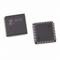
IC ENCORE MCU FLASH 32K 44PLCC
Manufacturer
Zilog
Series
Encore!®r
Datasheet
1.Z8F1601VN020EC.pdf
(246 pages)
Specifications of Z8F3201VN020EC00TR
Core Processor
Z8
Core Size
8-Bit
Speed
20MHz
Connectivity
I²C, IrDA, SPI, UART/USART
Peripherals
Brown-out Detect/Reset, DMA, POR, PWM, WDT
Number Of I /o
31
Program Memory Size
32KB (32K x 8)
Program Memory Type
FLASH
Ram Size
2K x 8
Voltage - Supply (vcc/vdd)
3 V ~ 3.6 V
Data Converters
A/D 8x10b
Oscillator Type
Internal
Operating Temperature
-40°C ~ 105°C
Package / Case
44-LCC (J-Lead)
Lead Free Status / RoHS Status
Contains lead / RoHS non-compliant
Eeprom Size
-
Other names
Z8F3201VN020EC00T
Available stocks
Company
Part Number
Manufacturer
Quantity
Price


PS017610-0404
SPI Signals
mitter and receiver sections, a Baud Rate (clock) Generator and a control unit. The trans-
mitter and receiver sections use the same clock.
During an SPI transfer, data is sent and received simultaneously by both the Master and
the Slave SPI devices. Separate signals are required for data and the serial clock. When an
SPI transfer occurs, a multi-bit (typically 8-bit) character is shifted out one data pin and an
multi-bit character is simultaneously shifted in on a second data pin. An 8-bit shift register
in the Master and another 8-bit shift register in the Slave are connected as a circular buffer.
The SPI shift register is single-buffered in the transmit and receive directions. New data to
be transmitted cannot be written into the shift register until the previous transmission is
complete and receive data (if valid) has been read.
The four basic SPI signals are:
•
•
•
•
The following paragraphs discuss these SPI signals. Each signal is described in both Mas-
ter and Slave modes.
Master-In, Slave-Out
The Master-In, Slave-Out (MISO) pin is configured as an input in a Master device and as
an output in a Slave device. It is one of the two lines that transfer serial data, with the most
significant bit sent first. The MISO pin of a Slave device is placed in a high-impedance
state if the Slave is not selected. When the SPI is not enabled, this signal is in a high-
impedance state.
Master-Out, Slave-In
The Master-Out, Slave-In (MOSI) pin is configured as an output in a Master device and as
an input in a Slave device. It is one of the two lines that transfer serial data, with the most
significant bit sent first. When the SPI is not enabled, this signal is in a high-impedance
state.
Serial Clock
The Serial Clock (SCK) is used to synchronize data movement both in and out of the
device through its MOSI and MISO pins. In Master mode, the SPI’s Baud Rate Generator
creates the serial clock. The Master drives the serial clock out its own SCK pin to the
Slave’s SCK pin. When the SPI is configured as a Slave, the SCK pin is an input and the
clock signal from the Master synchronizes the data transfer between the Master and Slave
devices. Slave devices ignore the SCK signal, unless the SS pin is asserted.
MISO (Master-In, Slave-Out)
MOSI (Master-Out, Slave-In)
SCK (SPI Serial Clock)
SS (Slave Select)
Z8F640x/Z8F480x/Z8F320x/Z8F240x/Z8F160x
Serial Peripheral Interface
Z8 Encore!
®
101
Related parts for Z8F3201VN020EC00TR
Image
Part Number
Description
Manufacturer
Datasheet
Request
R

Part Number:
Description:
Communication Controllers, ZILOG INTELLIGENT PERIPHERAL CONTROLLER (ZIP)
Manufacturer:
Zilog, Inc.
Datasheet:

Part Number:
Description:
KIT DEV FOR Z8 ENCORE 16K TO 64K
Manufacturer:
Zilog
Datasheet:

Part Number:
Description:
KIT DEV Z8 ENCORE XP 28-PIN
Manufacturer:
Zilog
Datasheet:

Part Number:
Description:
DEV KIT FOR Z8 ENCORE 8K/4K
Manufacturer:
Zilog
Datasheet:

Part Number:
Description:
KIT DEV Z8 ENCORE XP 28-PIN
Manufacturer:
Zilog
Datasheet:

Part Number:
Description:
DEV KIT FOR Z8 ENCORE 4K TO 8K
Manufacturer:
Zilog
Datasheet:
Part Number:
Description:
CMOS Z8 microcontroller. ROM 16 Kbytes, RAM 256 bytes, speed 16 MHz, 32 lines I/O, 3.0V to 5.5V
Manufacturer:
Zilog, Inc.
Datasheet:
Part Number:
Description:
Low-cost microcontroller. 512 bytes ROM, 61 bytes RAM, 8 MHz
Manufacturer:
Zilog, Inc.
Datasheet:
Part Number:
Description:
Z8 4K OTP Microcontroller
Manufacturer:
Zilog, Inc.
Datasheet:
Part Number:
Description:
CMOS SUPER8 ROMLESS MCU
Manufacturer:
Zilog, Inc.
Datasheet:
Part Number:
Description:
SL1866 CMOSZ8 OTP Microcontroller
Manufacturer:
Zilog, Inc.
Datasheet:
Part Number:
Description:
SL1866 CMOSZ8 OTP Microcontroller
Manufacturer:
Zilog, Inc.
Datasheet:
Part Number:
Description:
OTP (KB) = 1, RAM = 125, Speed = 12, I/O = 14, 8-bit Timers = 2, Comm Interfaces Other Features = Por, LV Protect, Voltage = 4.5-5.5V
Manufacturer:
Zilog, Inc.
Datasheet:
Part Number:
Description:
Manufacturer:
Zilog, Inc.
Datasheet: