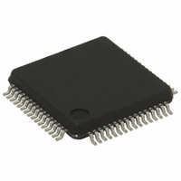
ST7FMC2R7T6TR STMicroelectronics, ST7FMC2R7T6TR Datasheet - Page 197

ST7FMC2R7T6TR
Manufacturer Part Number
ST7FMC2R7T6TR
Description
IC MCU 8BIT 32K FLASH 64-LQFP
Manufacturer
STMicroelectronics
Series
ST7r
Datasheet
1.ST7FMC2S4T6.pdf
(309 pages)
Specifications of ST7FMC2R7T6TR
Core Processor
ST7
Core Size
8-Bit
Speed
8MHz
Connectivity
LINSCI, SPI
Peripherals
LVD, Motor Control PWM, POR, PWM, WDT
Number Of I /o
44
Program Memory Size
48KB (48K x 8)
Program Memory Type
FLASH
Ram Size
1.5K x 8
Voltage - Supply (vcc/vdd)
3.8 V ~ 5.5 V
Data Converters
A/D 16x10b
Oscillator Type
Internal
Operating Temperature
-40°C ~ 85°C
Package / Case
64-LQFP
For Use With
497-8402 - BOARD EVAL COMPLETE INVERTER497-8400 - KIT IGBT PWR MODULE CTRL ST7MC497-6408 - BOARD EVAL BLDC SENSORLESS MOTOR497-4734 - EVAL KIT 3KW POWER DRIVER BOARD497-4733 - EVAL KIT 1KW POWER DRIVER BOARD497-4732 - EVAL KIT 300W POWER DRIVER BOARD497-4731 - EVAL KIT PWR DRIVER CONTROL BRD
Lead Free Status / RoHS Status
Lead free / RoHS Compliant
Eeprom Size
-
Available stocks
Company
Part Number
Manufacturer
Quantity
Price
Company:
Part Number:
ST7FMC2R7T6TR
Manufacturer:
STMicroelectronics
Quantity:
10 000
- Current page: 197 of 309
- Download datasheet (6Mb)
MOTOR CONTROLLER (Cont’d)
If the PCN bit is reset, one of the three PWM sig-
nals (the one set by the compare U register pair) or
the output of the measurement window generator
(depending on if the driving mode is voltage or cur-
rent) is used to provide six-step signals through
the PWM manager (to drive a PM BLDC motor for
instance).
In that case, DTE behaves like a standard bit (with
multiple write capability). When the deadtime gen-
erator is enabled (bit DTE=1), some restrictions
are applied, summarized in
■
■
■
Table 53
time generator when the PCN bit is reset. 1(pwm*)
means that the corresponding channel is active (1
in the corresponding bit in the MPHST register),
and a PWM signal is applied on it (using the MPAR
register and the OS[2:0] bits in MCRB register).
PWM represents the complementary signals (al-
though the duty cycle is slightly different due to
deadtime insertion). 0 means that the channel is
inactive and 1 means that the channel is active
and a logic level 1 is applied on it (no PWM signal).
Channels
Channel[0:1], Channel[2:3], Channel[4:5]; a
deadtime generator is allocated to each of these
pairs (see cautions below);
The input signal of the deadtime generator is the
active output of the PWM manager for the
corresponding channel. For instance, if we
consider the Channel[0:1] pair, it may be either
Channel0 or Channel1.
When both channels of a pair are inactive, the
corresponding outputs will also stay inactive
(this is mandatory to allow BEMF zero-crossing
detection).
summarizes the functionality of the dead-
are
now
Table
grouped
53:
by
pairs:
Table 53. Dead Time generator outputs
* PWM generation enabled
Warning: Grouping channels by pairs imposes the
external connections between the MCO outputs
and power devices; the user must therefore pay at-
tention to respect the “recommended schematics”
described in
124
Note: As soon as the channels are grouped in
pairs, special care has to be taken in configuring
the MPAR register for a PM BLDC drive. If both
channels of the same pair are both labelled “high”
for example and if the PWM is applied on high
channels, the active MCO output x (OOx=1 bit in
the MPHST register) outputs PWM and the paired
MCO output x+1 (OOx+1bit in the MPHST regis-
ter) outputs PWM and vice versa.
Caution: When PCN=0 and a complementary
PWM is applied (DTE=1) on one channel of a pair,
if both channels are active, this corresponds in
output to both channels OFF. This is for security
purpose to avoid cross-conduction.
Caution: To clear the DTE bit from reset state of
MDTG register (FFh), the PCN bit must be cleared
before.
(OOx bit)
1 (pwm*)
1 (pwm*)
On/Off x
0
1
1
0
0
PCN = 0; DTE =1; x= 0, 2, 4
(OOx+1 bit)
On/Off x+1
Figure 123. on page 228
1 (pwm*)
1 (pwm*)
0
1
0
1
0
ST7MC1xx/ST7MC2xx
MCOx output
PWM
PWM
0
0
1
0
0
and
MCOx+1
output
PWM
PWM
197/309
0
0
0
1
0
Figure
1
Related parts for ST7FMC2R7T6TR
Image
Part Number
Description
Manufacturer
Datasheet
Request
R

Part Number:
Description:
STMicroelectronics [RIPPLE-CARRY BINARY COUNTER/DIVIDERS]
Manufacturer:
STMicroelectronics
Datasheet:

Part Number:
Description:
STMicroelectronics [LIQUID-CRYSTAL DISPLAY DRIVERS]
Manufacturer:
STMicroelectronics
Datasheet:

Part Number:
Description:
BOARD EVAL FOR MEMS SENSORS
Manufacturer:
STMicroelectronics
Datasheet:

Part Number:
Description:
NPN TRANSISTOR POWER MODULE
Manufacturer:
STMicroelectronics
Datasheet:

Part Number:
Description:
TURBOSWITCH ULTRA-FAST HIGH VOLTAGE DIODE
Manufacturer:
STMicroelectronics
Datasheet:

Part Number:
Description:
Manufacturer:
STMicroelectronics
Datasheet:

Part Number:
Description:
DIODE / SCR MODULE
Manufacturer:
STMicroelectronics
Datasheet:

Part Number:
Description:
DIODE / SCR MODULE
Manufacturer:
STMicroelectronics
Datasheet:

Part Number:
Description:
Search -----> STE16N100
Manufacturer:
STMicroelectronics
Datasheet:

Part Number:
Description:
Search ---> STE53NA50
Manufacturer:
STMicroelectronics
Datasheet:

Part Number:
Description:
NPN Transistor Power Module
Manufacturer:
STMicroelectronics
Datasheet:

Part Number:
Description:
DIODE / SCR MODULE
Manufacturer:
STMicroelectronics
Datasheet:


