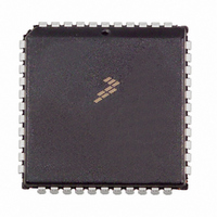
MC68HC711D3CFN2 Freescale Semiconductor, MC68HC711D3CFN2 Datasheet - Page 77

MC68HC711D3CFN2
Manufacturer Part Number
MC68HC711D3CFN2
Description
IC MCU 2MHZ 4K OTP 44-PLCC
Manufacturer
Freescale Semiconductor
Series
HC11r
Specifications of MC68HC711D3CFN2
Core Processor
HC11
Core Size
8-Bit
Speed
2MHz
Connectivity
SCI, SPI
Peripherals
POR, WDT
Number Of I /o
26
Program Memory Size
4KB (4K x 8)
Program Memory Type
OTP
Ram Size
192 x 8
Voltage - Supply (vcc/vdd)
4.5 V ~ 5.5 V
Oscillator Type
Internal
Operating Temperature
-40°C ~ 85°C
Package / Case
44-PLCC
Lead Free Status / RoHS Status
Contains lead / RoHS non-compliant
Eeprom Size
-
Data Converters
-
Available stocks
Company
Part Number
Manufacturer
Quantity
Price
Company:
Part Number:
MC68HC711D3CFN2
Manufacturer:
DIODES
Quantity:
12 000
Company:
Part Number:
MC68HC711D3CFN2
Manufacturer:
MOT
Quantity:
5 510
Company:
Part Number:
MC68HC711D3CFN2
Manufacturer:
Freescale Semiconductor
Quantity:
10 000
Chapter 7
Serial Peripheral Interface (SPI)
7.1 Introduction
The serial peripheral interface (SPI), an independent serial communications subsystem, allows the
microcontroller unit (MCU) to communicate synchronously with peripheral devices, such as:
The SPI is also capable of inter-processor communication in a multiple master system. The SPI system
can be configured as either a master or a slave device with data rates as high as one half of the E-clock
rate when configured as master, and as fast as the E-clock rate when configured as slave.
7.2 Functional Description
The central element in the SPI system is the block containing the shift register and the read data buffer.
The system is single buffered in the transmit direction and double buffered in the receive direction. This
means that new data for transmission cannot be written to the shifter until the previous transfer is
complete; however, received data is transferred into a parallel read data buffer so the shifter is free to
accept a second serial character. As long as the first character is read out of the read data buffer before
the next serial character is ready to be transferred, no overrun condition occurs. A single MCU register
address is used for reading data from the read data buffer, and for writing data to the shifter.
The SPI status block represents the SPI status functions (transfer complete, write collision, and mode
fault) performed by the serial peripheral status register (SPSR). The SPI control block represents those
functions that control the SPI system through the serial peripheral control register (SPCR).
Refer to
7.3 SPI Transfer Formats
During an SPI transfer, data is simultaneously transmitted and received. A serial clock line synchronizes
shifting and sampling of the information on the two serial data lines. A slave select line allows individual
selection of a slave SPI device; slave devices that are not selected do not interfere with SPI bus activities.
On a master SPI device, the select line can optionally be used to indicate a multiple master bus
contention. Refer to
Freescale Semiconductor
•
•
•
•
Transistor-transistor logic (TTL) shift registers
Liquid crystal diode (LCD) display drivers
Analog-to-digital converter (ADC) subsystems
Other microprocessors (MCUs)
Figure
7-1, which shows the SPI block diagram.
Figure
7-2.
MC68HC711D3 Data Sheet, Rev. 2.1
77


