HD6417032F20 Renesas Electronics America, HD6417032F20 Datasheet - Page 139
HD6417032F20
Manufacturer Part Number
HD6417032F20
Description
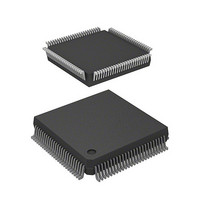
IC SUPERH MPU ROMLESS 112QFP
Manufacturer
Renesas Electronics America
Series
SuperH® SH7030r
Datasheet
1.HD6417034AFI20.pdf
(689 pages)
Specifications of HD6417032F20
Core Processor
SH-1
Core Size
32-Bit
Speed
20MHz
Connectivity
EBI/EMI, SCI
Peripherals
DMA, POR, PWM, WDT
Number Of I /o
32
Program Memory Type
ROMless
Ram Size
4K x 8
Voltage - Supply (vcc/vdd)
4.5 V ~ 5.5 V
Data Converters
A/D 8x10b
Oscillator Type
Internal
Operating Temperature
-20°C ~ 75°C
Package / Case
112-QFP
Lead Free Status / RoHS Status
Contains lead / RoHS non-compliant
Eeprom Size
-
Program Memory Size
-
Available stocks
Company
Part Number
Manufacturer
Quantity
Price
Company:

Part Number:
HD6417032F20
Manufacturer:
HIT
Quantity:
5 510
Company:
Part Number:
HD6417032F20
Manufacturer:
AMCC
Quantity:
5 510
Company:
Part Number:
HD6417032F20
Manufacturer:
Renesas Electronics America
Quantity:
10 000
Part Number:
HD6417032F20
Manufacturer:
HITACHI/日立
Quantity:
20 000
Company:
Part Number:
HD6417032F20V
Manufacturer:
TI
Quantity:
201


8.2.2
Wait state control register 1 is a 16-bit read/write register that controls the number of states for
accessing each area and whether wait states are used. WCR1 is initialized to H'FFFF by a power-
on reset. It is not initialized by a manual reset or in standby mode.
Bits 15–8—Wait State Control During Read (RW7–RW0): RW7–RW0 determine the number
of states in read cycles for each area and whether or not to sample the signal input from the WAIT
pin. Bits RW7–RW0 correspond to areas 7–0, respectively. If a bit is cleared to 0, the WAIT
signal is not sampled during the read cycle for the corresponding area. If it is set to 1, sampling
takes place.
For the external memory spaces of areas 1, 3–5, and 7, read cycles are completed in one state
when the corresponding bits are cleared to 0. When they are set to 1, the number of wait states is 2
plus the WAIT signal value. For the external memory space of areas 0, 2, and 6, read cycles are
completed in one state plus the number of long wait states (set in wait state controller 3 (WCR3))
when the corresponding bits are cleared to 0. When they are set to 1, the number of wait states is 1
plus the long wait state; when the WAIT signal is low as well, a wait state is inserted.
The DRAM space (area 1) finishes the column address output cycle in one state (short pitch) when
the RW1 bit is 0, and in 2 states plus the WAIT signal value (long pitch) when RW1 is 1. When
RW1 is set to 1, the number of wait states selected in wait state insertion bits 1 and 0 (RLW0 and
RLW1) for CAS-before-RAS (CBR) refresh in the refresh control register (RCR) are inserted
during the CBR refresh cycle, regardless of the status of the WAIT signal.
The read cycle of the address/data multiplexed I/O space (area 6) is 4 states plus the wait states
from the WAIT signal, regardless of the setting of the RW6 bit. The read cycle of the on-chip
supporting module space (area 5) finishes in 3 states, regardless of the setting of the RW5 bit, and
the WAIT signal is not sampled. The read cycles of on-chip ROM (area 0) and on-chip RAM (area
Bit
Initial value
Read/Write
Bit
Initial value
Read/Write
Wait State Control Register 1 (WCR1)
RW7
R/W
15
—
—
1
7
1
RW6
R/W
14
—
—
1
6
1
RW5
R/W
13
—
—
1
5
1
RW4
R/W
12
—
—
1
4
1
Rev. 7.00 Jan 31, 2006 page 111 of 658
Section 8 Bus State Controller (BSC)
RW3
R/W
11
—
—
1
3
1
RW2
R/W
10
—
—
1
2
1
REJ09B0272-0700
WW1
RW1
R/W
R/W
9
1
1
1
RW0
R/W
—
—
8
1
0
1
Related parts for HD6417032F20
Image
Part Number
Description
Manufacturer
Datasheet
Request
R

Part Number:
Description:
KIT STARTER FOR M16C/29
Manufacturer:
Renesas Electronics America
Datasheet:

Part Number:
Description:
KIT STARTER FOR R8C/2D
Manufacturer:
Renesas Electronics America
Datasheet:

Part Number:
Description:
R0K33062P STARTER KIT
Manufacturer:
Renesas Electronics America
Datasheet:

Part Number:
Description:
KIT STARTER FOR R8C/23 E8A
Manufacturer:
Renesas Electronics America
Datasheet:

Part Number:
Description:
KIT STARTER FOR R8C/25
Manufacturer:
Renesas Electronics America
Datasheet:

Part Number:
Description:
KIT STARTER H8S2456 SHARPE DSPLY
Manufacturer:
Renesas Electronics America
Datasheet:

Part Number:
Description:
KIT STARTER FOR R8C38C
Manufacturer:
Renesas Electronics America
Datasheet:

Part Number:
Description:
KIT STARTER FOR R8C35C
Manufacturer:
Renesas Electronics America
Datasheet:

Part Number:
Description:
KIT STARTER FOR R8CL3AC+LCD APPS
Manufacturer:
Renesas Electronics America
Datasheet:
Part Number:
Description:
KIT STARTER FOR RX610
Manufacturer:
Renesas Electronics America
Datasheet:

Part Number:
Description:
KIT STARTER FOR R32C/118
Manufacturer:
Renesas Electronics America
Datasheet:

Part Number:
Description:
KIT DEV RSK-R8C/26-29
Manufacturer:
Renesas Electronics America
Datasheet:

Part Number:
Description:
KIT STARTER FOR SH7124
Manufacturer:
Renesas Electronics America
Datasheet:

Part Number:
Description:
KIT STARTER FOR H8SX/1622
Manufacturer:
Renesas Electronics America
Datasheet:

Part Number:
Description:
KIT DEV FOR SH7203
Manufacturer:
Renesas Electronics America
Datasheet: