HD6417032F20 Renesas Electronics America, HD6417032F20 Datasheet - Page 146
HD6417032F20
Manufacturer Part Number
HD6417032F20
Description
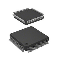
IC SUPERH MPU ROMLESS 112QFP
Manufacturer
Renesas Electronics America
Series
SuperH® SH7030r
Datasheet
1.HD6417034AFI20.pdf
(689 pages)
Specifications of HD6417032F20
Core Processor
SH-1
Core Size
32-Bit
Speed
20MHz
Connectivity
EBI/EMI, SCI
Peripherals
DMA, POR, PWM, WDT
Number Of I /o
32
Program Memory Type
ROMless
Ram Size
4K x 8
Voltage - Supply (vcc/vdd)
4.5 V ~ 5.5 V
Data Converters
A/D 8x10b
Oscillator Type
Internal
Operating Temperature
-20°C ~ 75°C
Package / Case
112-QFP
Lead Free Status / RoHS Status
Contains lead / RoHS non-compliant
Eeprom Size
-
Program Memory Size
-
Available stocks
Company
Part Number
Manufacturer
Quantity
Price
Company:

Part Number:
HD6417032F20
Manufacturer:
HIT
Quantity:
5 510
Company:
Part Number:
HD6417032F20
Manufacturer:
AMCC
Quantity:
5 510
Company:
Part Number:
HD6417032F20
Manufacturer:
Renesas Electronics America
Quantity:
10 000
Part Number:
HD6417032F20
Manufacturer:
HITACHI/日立
Quantity:
20 000
Company:
Part Number:
HD6417032F20V
Manufacturer:
TI
Quantity:
201


Section 8 Bus State Controller (BSC)
Bit 13—RAS Precharge Cycle Count (TPC): TPC selects whether the RAS signal precharge
cycle (T
when 1 is set, a 2-state precharge cycle is inserted.
Bit 13: TPC
0
1
Bit 12—Burst Operation Enable (BE): BE selects whether or not to perform burst operation, a
high-speed page mode. When burst operation is not selected (0), the row address is not compared
but instead is transferred to the DRAM every time and full access is performed. When burst
operation is selected (1), row addresses are compared and burst operation with the same row
address as previously is performed (in this access, no row address is output and the column
address and CAS signal alone are output) (high-speed page mode).
Bit 12: BE
0
1
Bit 11—CAS Duty (CDTY): CDTY selects 35% or 50% of the TC state as the high-level duty
ratio of the signal CAS in short-pitch access. When cleared to 0, the CAS signal high level duty is
50%; when set to 1, it is 35%.
Bit 11: CDTY
0
1
Bit 10—Multiplex Enable Bit (MXE): MXE determines whether or not DRAM row and column
addresses are multiplexed. When cleared to 0, addresses are not multiplexed; when set to 1, they
are multiplexed.
Bit 10: MXE
0
1
Rev. 7.00 Jan 31, 2006 page 118 of 658
REJ09B0272-0700
P
) will be 1 state or 2. When TPC is cleared to 0, a 1-state precharge cycle is inserted;
Description
1-state precharge cycle inserted
2-state precharge cycle inserted
Description
Normal mode: full access
Burst operation: high-speed page mode
Description
CAS signal high level duty cycle is 50% of the T
CAS signal high level duty cycle is 35% of the T
Description
Multiplexing of row and column addresses disabled
Multiplexing of row and column addresses enabled
C
C
state
state
(Initial value)
(Initial value)
(Initial value)
(Initial value)
Related parts for HD6417032F20
Image
Part Number
Description
Manufacturer
Datasheet
Request
R

Part Number:
Description:
KIT STARTER FOR M16C/29
Manufacturer:
Renesas Electronics America
Datasheet:

Part Number:
Description:
KIT STARTER FOR R8C/2D
Manufacturer:
Renesas Electronics America
Datasheet:

Part Number:
Description:
R0K33062P STARTER KIT
Manufacturer:
Renesas Electronics America
Datasheet:

Part Number:
Description:
KIT STARTER FOR R8C/23 E8A
Manufacturer:
Renesas Electronics America
Datasheet:

Part Number:
Description:
KIT STARTER FOR R8C/25
Manufacturer:
Renesas Electronics America
Datasheet:

Part Number:
Description:
KIT STARTER H8S2456 SHARPE DSPLY
Manufacturer:
Renesas Electronics America
Datasheet:

Part Number:
Description:
KIT STARTER FOR R8C38C
Manufacturer:
Renesas Electronics America
Datasheet:

Part Number:
Description:
KIT STARTER FOR R8C35C
Manufacturer:
Renesas Electronics America
Datasheet:

Part Number:
Description:
KIT STARTER FOR R8CL3AC+LCD APPS
Manufacturer:
Renesas Electronics America
Datasheet:
Part Number:
Description:
KIT STARTER FOR RX610
Manufacturer:
Renesas Electronics America
Datasheet:

Part Number:
Description:
KIT STARTER FOR R32C/118
Manufacturer:
Renesas Electronics America
Datasheet:

Part Number:
Description:
KIT DEV RSK-R8C/26-29
Manufacturer:
Renesas Electronics America
Datasheet:

Part Number:
Description:
KIT STARTER FOR SH7124
Manufacturer:
Renesas Electronics America
Datasheet:

Part Number:
Description:
KIT STARTER FOR H8SX/1622
Manufacturer:
Renesas Electronics America
Datasheet:

Part Number:
Description:
KIT DEV FOR SH7203
Manufacturer:
Renesas Electronics America
Datasheet: