LMC6024IM/NOPB National Semiconductor, LMC6024IM/NOPB Datasheet - Page 2
LMC6024IM/NOPB
Manufacturer Part Number
LMC6024IM/NOPB
Description
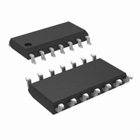
IC OP AMP QUAD LP CMOS 14-SOIC
Manufacturer
National Semiconductor
Datasheet
1.LMC6024IMNOPB.pdf
(14 pages)
Specifications of LMC6024IM/NOPB
Amplifier Type
General Purpose
Number Of Circuits
4
Output Type
Rail-to-Rail
Slew Rate
0.11 V/µs
Gain Bandwidth Product
350kHz
Current - Input Bias
0.04pA
Voltage - Input Offset
1000µV
Current - Supply
160µA
Current - Output / Channel
40mA
Voltage - Supply, Single/dual (±)
4.75 V ~ 15.5 V, ±2.38 V ~ 7.75 V
Operating Temperature
-40°C ~ 85°C
Mounting Type
Surface Mount
Package / Case
14-SOIC (3.9mm Width), 14-SOL
Number Of Channels
4
Voltage Gain Db
120 dB
Common Mode Rejection Ratio (min)
63 dB
Input Offset Voltage
9 mV at 5 V
Operating Supply Voltage
5 V, 9 V, 12 V, 15 V
Supply Current
0.24 mA at 5 V
Maximum Operating Temperature
+ 85 C
Maximum Dual Supply Voltage
+/- 7.75 V
Minimum Operating Temperature
- 40 C
Lead Free Status / RoHS Status
Lead free / RoHS Compliant
-3db Bandwidth
-
Lead Free Status / Rohs Status
Details
Other names
*LMC6024IM
*LMC6024IM/NOPB
LMC6024IM
*LMC6024IM/NOPB
LMC6024IM


www.national.com
V
∆V
I
I
R
CMRR
+PSRR
−PSRR
V
A
B
OS
Absolute Maximum Ratings
If Military/Aerospace specified devices are required,
please contact the National Semiconductor Sales Office/
Distributors for availability and specifications.
DC Electrical Characteristics
The following specifications apply for V
face limits apply at the temperature extremes; all other limits T
OS
IN
CM
V
Differential Input Voltage
Supply Voltage (V
Lead Temperature
Storage Temperature Range
Voltage at Output/Input Pin
Current at Input Pin
Current at Output Pin
Current at Power Supply Pin
Output Short Circuit to V
Symbol
OS
(Soldering, 10 sec.)
/∆T
Input Offset Voltage
Input Offset Voltage
Average Drift
Input Bias Current
Input Offset Current
Input Resistance
Common Mode
Rejection Ratio
Positive Power Supply
Rejection Ratio
Negative Power Supply
Rejection Ratio
Input Common-Mode
Voltage Range
Large Signal Voltage Gain
+
− V
−
)
+
Parameter
(V
+
) + 0.3V, (V
+
= 5V, V
−65˚C to +150˚C
±
Supply Voltage
(Note 1)
−
(Note 12)
−
= 0V, V
) − 0.3V
±
0V ≤ V
V
5V ≤ V
0V ≤ V
V
For CMRR ≥ 50 DB
R
Sourcing
Sinking
R
Sourcing
Sinking
±
18 mA
35 mA
+
+
L
L
260˚C
5 mA
= 15V
= 5V and 15V
= 100 kΩ (Note 7)
= 5 kΩ (Note 7)
16V
CM
+
−
CM
Conditions
≤ 15V
≤ −10V
≤ 12V
= 1.5V, V
2
J
= 25˚C.
Operating Ratings
Output Short Circuit to V
Junction Temperature
ESD Tolerance (Note 4)
Power Dissipation
Temperature Range
Supply Voltage Range
Power Dissipation
Thermal Resistance (θ
14-Pin DIP
14-Pin SO
O
= 2.5V, and R
V
(Note 5)
Typical
+
1000
1000
0.04
0.01
−0.4
500
250
L
2.5
>
83
83
94
− 1.9
1
= 1M unless otherwise noted. Bold-
1
JA
−
), (Note 11)
LMC6024I
V
V
(Note 6)
Limit
+
+
−0.1
200
100
200
100
100
11
63
61
63
61
74
73
90
40
75
50
20
− 2.3
− 2.5
9
0
4.75V to 15.5V
−40˚C ≤ T
(Note 10)
115˚C/W
(Note 2)
(Note 3)
85˚C/W
1000V
TeraΩ
+85˚C
Units
µV/˚C
150˚C
V/mV
V/mV
V/mV
V/mV
Max
Max
Max
Max
mV
Min
Min
Min
Min
Min
Min
Min
Min
pA
pA
dB
dB
dB
V
V
J
≤
Related parts for LMC6024IM/NOPB
Image
Part Number
Description
Manufacturer
Datasheet
Request
R

Part Number:
Description:
IC, OP-AMP, 350KHZ, 0.11V/µs, SOIC-14
Manufacturer:
National Semiconductor
Datasheet:

Part Number:
Description:
National Semiconductor [8-Bit D/A Converter]
Manufacturer:
National Semiconductor
Datasheet:
Part Number:
Description:
National Semiconductor [Media Coprocessor]
Manufacturer:
National Semiconductor
Datasheet:
Part Number:
Description:
Digitally Controlled Tone and Volume Circuit with Stereo Audio Power Amplifier, Microphone Preamp Stage and National 3D Sound
Manufacturer:
National Semiconductor
Datasheet:
Part Number:
Description:
Digitally Controlled Tone and Volume Circuit with Stereo Audio Power Amplifier, Microphone Preamp Stage and National 3D Sound
Manufacturer:
National Semiconductor
Datasheet:
Part Number:
Description:
AC97 Rev 2 Codec with Sample Rate Conversion and National 3D Sound
Manufacturer:
National Semiconductor
Part Number:
Description:
Manufacturer:
National Semiconductor
Datasheet:
Part Number:
Description:
Manufacturer:
National Semiconductor
Datasheet:
Part Number:
Description:
General Purpose, Low Voltage, Low Power, Rail-to-Rail Output Operational Amplifiers
Manufacturer:
National Semiconductor
Datasheet:
Part Number:
Description:
8-bit 20 MSPS flash A/D converter.
Manufacturer:
National Semiconductor
Datasheet:
Part Number:
Description:
Low Noise Quad Operational Amplifier
Manufacturer:
National Semiconductor
Datasheet:
Part Number:
Description:
Quad Differential Line Receivers
Manufacturer:
National Semiconductor
Datasheet:
Part Number:
Description:
Quad High Speed Trapezoidal? Bus Transceiver
Manufacturer:
National Semiconductor
Datasheet:
Part Number:
Description:
Dual Line Receiver
Manufacturer:
National Semiconductor
Datasheet: