LMC6024IM/NOPB National Semiconductor, LMC6024IM/NOPB Datasheet - Page 4
LMC6024IM/NOPB
Manufacturer Part Number
LMC6024IM/NOPB
Description
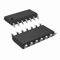
IC OP AMP QUAD LP CMOS 14-SOIC
Manufacturer
National Semiconductor
Datasheet
1.LMC6024IMNOPB.pdf
(14 pages)
Specifications of LMC6024IM/NOPB
Amplifier Type
General Purpose
Number Of Circuits
4
Output Type
Rail-to-Rail
Slew Rate
0.11 V/µs
Gain Bandwidth Product
350kHz
Current - Input Bias
0.04pA
Voltage - Input Offset
1000µV
Current - Supply
160µA
Current - Output / Channel
40mA
Voltage - Supply, Single/dual (±)
4.75 V ~ 15.5 V, ±2.38 V ~ 7.75 V
Operating Temperature
-40°C ~ 85°C
Mounting Type
Surface Mount
Package / Case
14-SOIC (3.9mm Width), 14-SOL
Number Of Channels
4
Voltage Gain Db
120 dB
Common Mode Rejection Ratio (min)
63 dB
Input Offset Voltage
9 mV at 5 V
Operating Supply Voltage
5 V, 9 V, 12 V, 15 V
Supply Current
0.24 mA at 5 V
Maximum Operating Temperature
+ 85 C
Maximum Dual Supply Voltage
+/- 7.75 V
Minimum Operating Temperature
- 40 C
Lead Free Status / RoHS Status
Lead free / RoHS Compliant
-3db Bandwidth
-
Lead Free Status / Rohs Status
Details
Other names
*LMC6024IM
*LMC6024IM/NOPB
LMC6024IM
*LMC6024IM/NOPB
LMC6024IM


www.national.com
SR
GBW
θ
G
e
i
n
M
n
AC Electrical Characteristics
The following specifications apply for V
face limits apply at the temperature extremes; all other limits T
Note 1: Absolute Maximum Ratings indicate limits beyond which damage to the component may occur. Operating Ratings indicate conditions for which the device
is intended to be functional, but do not guarantee specific performance limits. For guaranteed specifications and test conditions, see the Electrical Characteristics.
The guaranteed specifications apply only for the test conditions listed.
Note 2: Applies to both single-supply and split-supply operation. Continuous short circuit operation at elevated ambient temperature and/or multiple Op Amp shorts
can result in exceeding the maximum allowed junction temperature of 150˚C. Output currents in excess of
Note 3: The maximum power dissipation is a function of T
− T
Note 4: Human body model, 100 pF discharge through a 1.5 kΩ resistor.
Note 5: Typical values represent the most likely parametric norm.
Note 6: All limits are guaranteed by testing or correlation.
Note 7: V
Note 8: V
Note 9: Input referred, V
Note 10: For operating at elevated temperatures the device must be derated based on the thermal resistance θ
Note 11: All numbers apply for packages soldered directly into a PC board.
Note 12: Do not connect output to V
M
Symbol
A
)/θ
JA
.
+
+
= 15V, V
= 15V. Connected as Voltage Follower with 10V step input. Number specified is the slower of the positive and negative slew rates.
Slew Rate
Gain-Bandwidth Product
Phase Margin
Gain Margin
Amp-to-Amp Isolation
Input-Referred Voltage Noise
Input-Referred Current Noise
CM
= 7.5V, and R
+
= 15V and R
Parameter
+
L
when V
connected to 7.5V. For Sourcing tests, 7.5V ≤ V
L
= 100 kΩ connected to 7.5V. Each amp excited in turn with 1 kHz to produce V
+
is greater than 13V or reliability may be adversely affected.
+
= 5V, V
J(max)
−
, θ
= 0V, V
JA
(Note 8)
(Note 9)
F = 1 kHz
F = 1 kHz
, and T
Conditions
CM
A
. The maximum allowable power dissipation at any ambient temperature is P
= 1.5V, V
4
J
= 25˚C.
O
O
≤ 11.5V. For Sinking tests, 2.5V ≤ V
= 2.5V, and R
(Note 5)
Typical
0.0002
0.11
0.35
130
50
17
42
±
30 mA over long term may adversly affect reliability.
L
JA
= 1M unless otherwise noted. Bold-
with P
LMC6024I
(Note 6)
Limit
O
D
0.05
0.03
= 13 V
= (T
O
J
≤ 7.5V.
− T
PP
.
A
)/θ
JA
.
Units
V/µs
MHz
Deg
Min
dB
dB
D
= (T
J(max)
Related parts for LMC6024IM/NOPB
Image
Part Number
Description
Manufacturer
Datasheet
Request
R

Part Number:
Description:
IC, OP-AMP, 350KHZ, 0.11V/µs, SOIC-14
Manufacturer:
National Semiconductor
Datasheet:

Part Number:
Description:
National Semiconductor [8-Bit D/A Converter]
Manufacturer:
National Semiconductor
Datasheet:
Part Number:
Description:
National Semiconductor [Media Coprocessor]
Manufacturer:
National Semiconductor
Datasheet:
Part Number:
Description:
Digitally Controlled Tone and Volume Circuit with Stereo Audio Power Amplifier, Microphone Preamp Stage and National 3D Sound
Manufacturer:
National Semiconductor
Datasheet:
Part Number:
Description:
Digitally Controlled Tone and Volume Circuit with Stereo Audio Power Amplifier, Microphone Preamp Stage and National 3D Sound
Manufacturer:
National Semiconductor
Datasheet:
Part Number:
Description:
AC97 Rev 2 Codec with Sample Rate Conversion and National 3D Sound
Manufacturer:
National Semiconductor
Part Number:
Description:
Manufacturer:
National Semiconductor
Datasheet:
Part Number:
Description:
Manufacturer:
National Semiconductor
Datasheet:
Part Number:
Description:
General Purpose, Low Voltage, Low Power, Rail-to-Rail Output Operational Amplifiers
Manufacturer:
National Semiconductor
Datasheet:
Part Number:
Description:
8-bit 20 MSPS flash A/D converter.
Manufacturer:
National Semiconductor
Datasheet:
Part Number:
Description:
Low Noise Quad Operational Amplifier
Manufacturer:
National Semiconductor
Datasheet:
Part Number:
Description:
Quad Differential Line Receivers
Manufacturer:
National Semiconductor
Datasheet:
Part Number:
Description:
Quad High Speed Trapezoidal? Bus Transceiver
Manufacturer:
National Semiconductor
Datasheet:
Part Number:
Description:
Dual Line Receiver
Manufacturer:
National Semiconductor
Datasheet: