LMC6024IM/NOPB National Semiconductor, LMC6024IM/NOPB Datasheet - Page 9

LMC6024IM/NOPB
Manufacturer Part Number
LMC6024IM/NOPB
Description
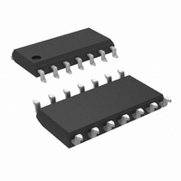
IC OP AMP QUAD LP CMOS 14-SOIC
Manufacturer
National Semiconductor
Datasheet
1.LMC6024IMNOPB.pdf
(14 pages)
Specifications of LMC6024IM/NOPB
Amplifier Type
General Purpose
Number Of Circuits
4
Output Type
Rail-to-Rail
Slew Rate
0.11 V/µs
Gain Bandwidth Product
350kHz
Current - Input Bias
0.04pA
Voltage - Input Offset
1000µV
Current - Supply
160µA
Current - Output / Channel
40mA
Voltage - Supply, Single/dual (±)
4.75 V ~ 15.5 V, ±2.38 V ~ 7.75 V
Operating Temperature
-40°C ~ 85°C
Mounting Type
Surface Mount
Package / Case
14-SOIC (3.9mm Width), 14-SOL
Number Of Channels
4
Voltage Gain Db
120 dB
Common Mode Rejection Ratio (min)
63 dB
Input Offset Voltage
9 mV at 5 V
Operating Supply Voltage
5 V, 9 V, 12 V, 15 V
Supply Current
0.24 mA at 5 V
Maximum Operating Temperature
+ 85 C
Maximum Dual Supply Voltage
+/- 7.75 V
Minimum Operating Temperature
- 40 C
Lead Free Status / RoHS Status
Lead free / RoHS Compliant
-3db Bandwidth
-
Lead Free Status / Rohs Status
Details
Other names
*LMC6024IM
*LMC6024IM/NOPB
LMC6024IM
*LMC6024IM/NOPB
LMC6024IM
Application Hints
AMPLIFIER TOPOLOGY
The topology chosen for the LMC6024 is unconventional
(compared to general-purpose op amps) in that the tradi-
tional unity-gain buffer output stage is not used; instead, the
output is taken directly from the output of the integrator, to
allow rail-to-rail output swing. Since the buffer traditionally
delivers the power to the load, while maintaining high op
amp gain and stability, and must withstand shorts to either
rail, these tasks now fall to the integrator.
As a result of these demands, the integrator is a compound
affair with an embedded gain stage that is doubly fed forward
(via C
driver. In addition, the output portion of the integrator is a
push-pull configuration for delivering heavy loads. While
sinking current the whole amplifier path consists of three
gain stages with one stage fed forward, whereas while
sourcing the path contains four gain stages with two fed
forward.
The large signal voltage gain while sourcing is comparable
to traditional bipolar op amps, for load resistance of at least
5 kΩ. The gain while sinking is higher than most CMOS op
amps, due to the additional gain stage; however, when driv-
ing load resistance of 5 kΩ or less, the gain will be reduced
as indicated in the Electrical Characterisitics. The op amp
can drive load resistance as low as 500Ω without instability.
COMPENSATING INPUT CAPACITANCE
Refer to the LMC660 or LMC662 datasheets to determine
whether or not a feedback capacitor will be necessary for
compensation and what the value of that capacitor would be.
CAPACITIVE LOAD TOLERANCE
Like many other op amps, the LMC6024 may oscillate when
its applied load appears capacitive. The threshold of oscilla-
tion varies both with load and circuit gain. The configuration
most sensitive to oscillation is a unity-gain follower. See the
Typical Performance Characteristics.
The load capacitance interacts with the op amp’s output
resistance to create an additional pole. If this pole frequency
is sufficiently low, it will degrade the op amp’s phase margin
so that the amplifier is no longer stable at low gains. The
addition of a small resistor (50Ω to 100Ω) in series with the
op amp’s output, and a capacitor (5 pF to 10 pF) from
inverting input to output pins, returns the phase margin to a
safe value without interfering with lower-frequency circuit
operation. Thus, larger values of capacitance can be toler-
FIGURE 1. LMC6024 Circuit Topology (Each Amplifier)
f
and C
ff
) by a dedicated unity-gain compensation
01123506
9
ated without oscillation. Note that in all cases, the output will
ring heavily when the load capcitance is near the threshold
for oscillation.
Capacitive load driving capability is enhanced by using a pull
up resistor to V
ducting 50 µA or more will significantly improve capacitive
load responses. The value of the pull up resistor must be
determined based on the current sinking capability of the
amplifier with respect to the desired output swing. Open loop
gain of the amplifier can also be affected by the pull up
resistor (see Electrical Characteristics).
PRINTED-CIRCUIT-BOARD LAYOUT
FOR HIGH-IMPEDANCE WORK
It is generally recognized that any circuit which must operate
with less than 1000 pA of leakage current requires special
layout of the PC board. When one wishes to take advantage
of the ultra-low bias current of the LMC6024, typically less
than 0.04 pA, it is essential to have an excellent layout.
Fortunately, the techniques for obtaining low leakages are
quite simple. First, the user must not ignore the surface
leakage of the PC board, even though it may sometimes
appear acceptably low, because under conditions of high
humidity or dust or contamination, the surface leakage will
be appreciable.
To minimize the effect of any surface leakage, lay out a ring
of foil completely surrounding the LMC6024’s inputs and the
terminals of capacitors, diodes, conductors, resistors, relay
terminals, etc. connected to the op-amp’s inputs. See Figure
4. To have a significant effect, guard rings should be placed
on both the top and bottom of the PC board. This PC foil
must then be connected to a voltage which is at the same
voltage as the amplifier inputs, since no leakage current can
flow between two points at the same potential. For example,
a PC board trace-to-pad resistance of 10
normally considered a very large resistance, could leak 5 pA
if the trace were a 5V bus adjacent to the pad of an input.
FIGURE 2. Rx, Cx Improve Capacitive Load Tolerance
Capacitive Loads with a Pull Up Resistor
FIGURE 3. Compensating for Large
+
Figure 3. Typically a pull up resistor con-
01123526
12
ohms, which is
01123507
www.national.com


